
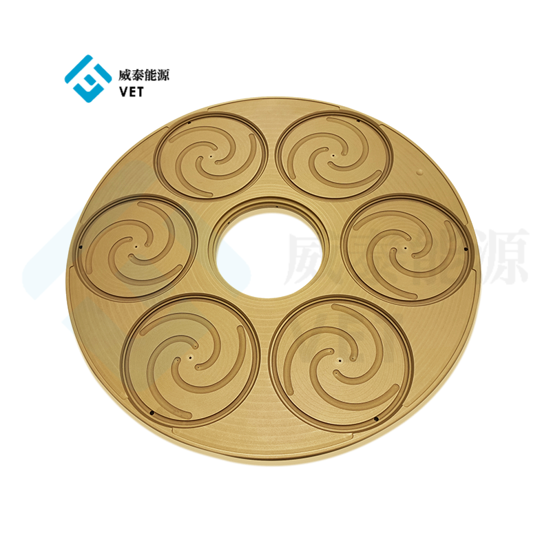
CVD TaC Coating Technology applies tantalum carbide coatings through chemical vapor deposition. This process enhances material durability and performance under extreme conditions. Industries rely on this innovation to achieve superior heat resistance and chemical stability. By bridging material science and industrial needs, it transforms manufacturing capabilities across high-performance sectors.
Key Takeaways
- CVD TaC Coating makes materials stronger and work better. It is great for tough jobs in industries like airplanes and computer chips.
- This coating handles heat well and resists chemicals. It helps parts last longer, lowers repair costs, and works more efficiently.
- New methods make the coating even and with fewer flaws. This ensures it works well in hard conditions.
Fundamentals of CVD TaC Coating
What is CVD TaC Coating?
CVD TaC Coating refers to a specialized process for applying tantalum carbide (TaC) layers onto substrates. This technology enhances the surface properties of materials, making them more durable and resistant to extreme conditions. Tantalum carbide, known for its exceptional hardness and thermal stability, forms a protective barrier that improves the performance of components in demanding environments. Industries adopt this coating to extend the lifespan of tools and equipment while maintaining efficiency.
Chemical Vapor Deposition Process
The chemical vapor deposition (CVD) process involves the reaction of gaseous precursors to deposit a thin film of material on a substrate. In the case of CVD TaC Coating, tantalum and carbon-containing gases react at high temperatures to form a uniform layer of tantalum carbide. This process ensures precise control over the coating’s thickness and composition. Manufacturers rely on this method for its ability to produce coatings with excellent adhesion and minimal defects.
Properties of Tantalum Carbide (TaC)
Tantalum carbide exhibits remarkable properties that make it ideal for high-performance applications. It has an extremely high melting point, exceeding 3,800°C, and exceptional hardness, ranking close to diamond on the Mohs scale. Its chemical inertness provides resistance to corrosion and oxidation, even in harsh environments. These characteristics make TaC coatings indispensable in industries requiring materials that can withstand extreme heat, pressure, and chemical exposure.
Material Science Innovations in CVD TaC Coating
Advances in Deposition Techniques
Material scientists have made significant progress in refining deposition techniques for CVD TaC Coating. Modern advancements focus on achieving uniform coatings with minimal defects. Researchers have optimized gas flow dynamics and reaction parameters to enhance the precision of the chemical vapor deposition process. These improvements allow manufacturers to produce coatings with consistent thickness and superior adhesion. Additionally, innovations in multi-layer deposition enable the creation of composite coatings that combine the properties of tantalum carbide with other materials. This approach enhances the versatility of CVD TaC Coating, making it suitable for a broader range of industrial applications.
High-Temperature and Corrosion Resistance
Tantalum carbide’s ability to withstand extreme conditions makes it a preferred choice for high-performance coatings. CVD TaC Coating exhibits exceptional resistance to high temperatures, maintaining structural integrity even beyond 3,800°C. This property ensures reliable performance in environments such as furnaces, reactors, and aerospace components. Furthermore, its chemical inertness protects substrates from corrosive agents, including acids and alkalis. These characteristics reduce material degradation, extending the lifespan of coated components. Industries benefit from this combination of heat and corrosion resistance, which minimizes maintenance costs and improves operational efficiency.
Overcoming Material Challenges
Developing effective CVD TaC Coating involves addressing several material challenges. One key issue is achieving a defect-free coating on complex geometries. Researchers have introduced advanced precursor materials and deposition techniques to overcome this limitation. Another challenge lies in managing the thermal stresses that arise during the coating process. By fine-tuning deposition parameters, scientists have minimized these stresses, ensuring better adhesion and durability. These innovations demonstrate how material science continues to push the boundaries of what is possible with CVD TaC Coating.
Industrial Applications of CVD TaC Coating
Semiconductor Manufacturing
CVD TaC Coating plays a critical role in semiconductor manufacturing. The coating’s exceptional thermal stability and chemical resistance make it ideal for protecting components in plasma etching and deposition equipment. These processes often involve exposure to corrosive gases and extreme temperatures. Tantalum carbide coatings ensure the longevity and reliability of critical parts, such as wafer carriers and chamber linings. By reducing wear and contamination, the technology enhances the precision and efficiency of semiconductor fabrication.
SiC and AlN Crystal Growth
The production of silicon carbide (SiC) and aluminum nitride (AlN) crystals requires materials that can withstand high temperatures and aggressive chemical environments. CVD TaC Coating provides the necessary protection for graphite components used in these processes. Its ability to resist oxidation and maintain structural integrity ensures consistent crystal growth. This reliability is essential for producing high-quality materials used in power electronics and optoelectronics. Manufacturers benefit from reduced maintenance and improved yield rates, making the coating indispensable in this field.
Aerospace and High-Performance Industries
Aerospace and other high-performance industries demand materials capable of enduring extreme conditions. CVD TaC Coating offers unparalleled heat resistance, making it suitable for applications such as rocket nozzles, turbine blades, and heat shields. Its chemical inertness also protects components from corrosive fuels and oxidizers. These properties enhance the durability and performance of critical systems, ensuring safety and efficiency in demanding environments.
Benefits: Durability, Efficiency, and Chemical Resistance
The benefits of CVD TaC Coating extend across multiple industries. Its durability reduces the frequency of component replacement, lowering operational costs. The coating’s efficiency improves energy utilization by maintaining performance under extreme conditions. Its chemical resistance minimizes the risk of contamination and degradation, ensuring consistent operation. These advantages make it a valuable solution for industries seeking to optimize performance and reliability.
CVD TaC coating technology has revolutionized material science by enhancing durability, heat resistance, and chemical stability. Its industrial applications demonstrate its transformative impact on manufacturing processes. This innovation holds immense potential to drive advancements in aerospace, semiconductors, and other high-performance sectors, paving the way for groundbreaking developments in advanced manufacturing and engineering.
FAQ
What industries benefit the most from CVD TaC coating technology?
Industries like aerospace, semiconductors, and crystal growth benefit significantly. The coating enhances durability, heat resistance, and chemical stability in extreme operational environments.
How does CVD TaC coating improve component lifespan?
The coating protects components from wear, corrosion, and thermal stress. Its exceptional hardness and chemical inertness reduce degradation, extending operational life.
Is CVD TaC coating environmentally sustainable?
CVD TaC coating minimizes material waste by extending component life. Its precise application process reduces resource consumption, supporting sustainable manufacturing practices.

