
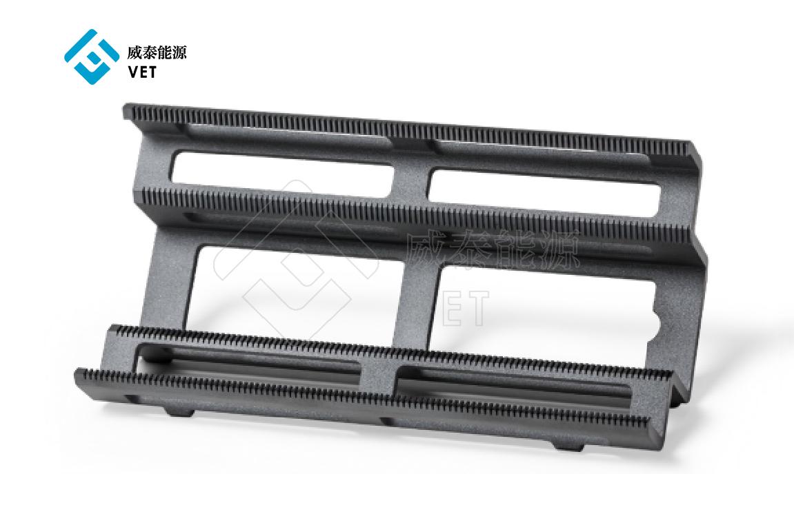
The Contiguous Wafer Boat from vet-china transforms semiconductor manufacturing in 2025. Its advanced design ensures precise wafer handling, boosting efficiency and reliability. A major fab reported a 15% yield increase, while another reduced downtime by 20%. This innovation, crafted with durable materials like the Silicon Carbide Boat, meets the demands of modern fabs. The contiguous boat design enhances operational performance, making the contiguous wafer boat an essential tool for any semiconductor manufacturer.
Key Takeaways
- The Contiguous Wafer Boat makes chip-making faster and safer. It has locks to hold wafers tightly and stop damage.
- Easy-release designs help load and unload wafers quickly. This saves time and lowers mistakes, making work smoother.
- Makers can change the wafer boat to fit their needs. This improves how wafers line up and speeds up work in busy factories.
Key Features and Benefits of the Contiguous Wafer Boat
Self-locking Mechanisms for Secure Wafer Handling
The Contiguous Wafer Boat incorporates advanced self-locking mechanisms that ensure wafers remain securely in place during manufacturing. This feature minimizes unintended movement, which reduces the risk of physical damage such as scratches or cracks. By maintaining precise alignment, the self-locking mechanism enhances operational reliability and prevents errors caused by misalignment.
| Feature | Benefit | Impact on Reliability |
|---|---|---|
| Self-locking Mechanism | Secures wafers firmly in place, preventing unintended movement | Enhances operational reliability |
| Stability | Maintains precise alignment during manufacturing processes | Minimizes errors caused by misalignment |
| Damage Prevention | Protects wafers from scratches, cracks, or defects | Contributes to higher yield rates |
| Cost Efficiency | Reduces the number of rejected wafers, leading to cost savings | Improves overall manufacturing efficiency |
Quick-release Designs for Enhanced Efficiency
The quick-release design of the Contiguous Wafer Boat streamlines wafer handling, making loading and unloading faster and more efficient. This feature significantly reduces production time, allowing manufacturers to optimize workflows. By facilitating easier handling, the quick-release design also minimizes the risk of human error, further improving manufacturing efficiency. Many fabs have reported smoother operations and reduced downtime after integrating this innovative design.
- Key Benefits of Quick-release Design:
- Faster wafer loading and unloading.
- Reduced production time and improved workflow.
- Lower risk of handling errors.
High-temperature Resistance for Extreme Manufacturing Conditions
The Contiguous Wafer Boat demonstrates exceptional high-temperature resistance, making it ideal for processes like thermal oxidation and annealing. Its structural integrity remains intact even under prolonged exposure to intense heat, ensuring consistent performance. Accelerated Life Testing (ALT) and High-Temperature Operating Life (HTOL) tests confirm its durability in extreme conditions, providing manufacturers with a reliable tool for critical semiconductor processes.
| Property | Description |
|---|---|
| High-Temperature Resistance | The Contiguous Wafer Boat remains stable and reliable in extreme thermal conditions, ensuring consistent performance in semiconductor processes. |
| Structural Integrity | Maintains integrity during prolonged exposure to intense heat, critical for processes like thermal oxidation and annealing. |
The Contiguous Wafer Boat’s ability to withstand extreme environments ensures long-term reliability and supports the demanding needs of modern semiconductor fabs.
Material Advantages of the Contiguous Wafer Boat
Quartz: A Cost-effective and Reliable Option
Quartz offers a practical and economical solution for semiconductor manufacturing. Its excellent thermal stability ensures consistent performance during high-temperature processes. Manufacturers value quartz for its ability to resist chemical corrosion, making it suitable for environments with aggressive chemicals. Additionally, quartz is lightweight, which simplifies handling and reduces strain on equipment. These qualities make it a reliable material for the Contiguous Wafer Boat, especially in applications requiring precision and durability.
Silicon Carbide (SiC): Superior Strength and Thermal Conductivity
Silicon Carbide (SiC) stands out due to its remarkable strength and thermal conductivity. These properties make it an ideal choice for demanding semiconductor processes. SiC ensures efficient heat distribution, which is critical for maintaining uniform temperatures during wafer processing. Its high flexural strength and fracture toughness provide exceptional durability, even under mechanical stress. The table below highlights SiC’s key properties:
| Property | Value |
|---|---|
| Thermal Conductivity | 120 W/m•K |
| Flexural Strength | 490 MPa |
| Fracture Toughness | 6.8 MPa m0.5 |
| Young’s Modulus | 440 GPa |
These attributes demonstrate why SiC is a superior material for the Contiguous Wafer Boat, ensuring reliability and efficiency in semiconductor manufacturing.
R-SiC: Advanced Durability and Longevity
R-SiC offers unmatched durability and longevity, making it a preferred material for critical manufacturing applications. Its exceptional corrosion resistance allows it to perform reliably in chemically aggressive environments. R-SiC also withstands extreme temperatures without losing structural integrity, ensuring consistent performance over time. These advanced properties make R-SiC an excellent choice for manufacturers seeking long-lasting solutions. By incorporating R-SiC into the Contiguous Wafer Boat, manufacturers can enhance operational efficiency and reduce maintenance costs.
Customization Options for the Contiguous Wafer Boat
Design Flexibility for Unique Manufacturing Needs
The Contiguous Wafer Boat offers exceptional design flexibility, allowing manufacturers to tailor its size and shape to meet specific wafer dimensions. This customization ensures precise wafer alignment, reducing the risk of misalignment and improving overall production accuracy. Additionally, manufacturers can opt for color-coded wafer boats to streamline identification and organization in complex production environments. This feature enhances workflow efficiency by simplifying the management of multiple wafer boats. Specialized coatings are also available, providing increased durability and chemical resistance. These coatings extend the product’s lifespan and reduce maintenance costs, making the wafer boat a cost-effective solution.
| Feature | Description |
|---|---|
| Design Flexibility | Customizable size and shape for precise wafer alignment. |
| Color Coding | Simplifies identification and organization in complex setups. |
| Specialized Coatings | Enhances durability and chemical resistance, reducing maintenance costs. |
Integrated Sensors for Real-time Monitoring
Integrated sensors in the Contiguous Wafer Boat enable real-time monitoring of critical wafer conditions. These sensors collect data on parameters such as temperature and alignment, ensuring consistent quality throughout the manufacturing process. By providing immediate feedback, the sensors help manufacturers detect and address potential issues before they escalate. This capability reduces defects and enhances process control, resulting in higher yield rates. Real-time monitoring also supports predictive maintenance, minimizing downtime and improving operational efficiency.
- Key benefits of integrated sensors:
- Real-time data collection on temperature and alignment.
- Enhanced process control for consistent quality.
- Reduced defects and improved yield rates.
Additional Features for Enhanced Performance
The Contiguous Wafer Boat includes additional features designed to optimize performance in semiconductor manufacturing. Modular designs allow for quick adjustments, accommodating changes in production requirements. Anti-static properties prevent the buildup of static electricity, protecting wafers from potential damage. Furthermore, advanced thermal management systems ensure uniform heat distribution, critical for high-temperature processes. These features collectively enhance the wafer boat’s reliability and adaptability, making it an indispensable tool for modern fabs.
Maintenance and Complementary Tools for the Contiguous Wafer Boat
Tools for Safe Handling and Transport
Proper handling and transport tools are essential for maintaining the integrity of the Contiguous Wafer Boat. These tools minimize risks during movement and storage, ensuring wafers remain undamaged. Manufacturers often rely on padded carriers and anti-static containers to protect the wafer boat from physical shocks and static discharge. Additionally, automated handling systems reduce human interaction, lowering the chances of mishandling.
Safety data highlights the importance of using effective tools. For instance:
- Crash data analysis shows how safety measures reduce risks in critical situations.
- Countermeasure effectiveness studies reveal the benefits of protective tools in minimizing damage.
- Nationwide statistics emphasize the role of proper handling in preventing costly accidents.
These insights underline the importance of investing in high-quality handling tools to safeguard wafer boats during transport.
Importance of Regular Cleaning and Maintenance
Routine cleaning and maintenance ensure the Contiguous Wafer Boat performs optimally. Residue buildup from manufacturing processes can compromise wafer alignment and thermal conductivity. Using non-abrasive cleaning agents and specialized brushes helps remove contaminants without damaging the boat’s surface. Regular inspections also identify wear and tear early, preventing costly replacements. A well-maintained wafer boat enhances production efficiency and extends its lifespan.
Partnering with vet-china for Support and Solutions
Vet-china provides comprehensive support for maintaining the Contiguous Wafer Boat. Their expert team offers guidance on best practices for cleaning, handling, and storage. Additionally, they supply complementary tools designed to maximize the wafer boat’s performance. By partnering with vet-china, manufacturers gain access to tailored solutions that address their unique operational needs. This collaboration ensures long-term reliability and efficiency in semiconductor manufacturing.
The Contiguous Wafer Boat from vet-china continues to redefine semiconductor manufacturing in 2025 and beyond. Its innovative features and durable materials ensure precision and efficiency. Future projections highlight its critical role in the industry:
| Metric | Improvement |
|---|---|
| Yield Rate Increase | 15% |
| Downtime Reduction | 20% |
- Automation enhances efficiency and reduces human error.
- Sustainability drives demand for energy-efficient wafer boats.
- The need for smaller, powerful chips requires precise wafer handling.
Advancements in thermal stability and alignment capabilities will further optimize production, ensuring adaptability to evolving market demands.
FAQ
What makes the Contiguous Wafer Boat unique compared to traditional wafer boats?
The Contiguous Wafer Boat offers advanced features like self-locking mechanisms, high-temperature resistance, and customizable designs. These innovations improve wafer handling, enhance efficiency, and ensure long-term reliability.
Can the Contiguous Wafer Boat handle different wafer sizes?
Yes, the Contiguous Wafer Boat supports various wafer sizes. Its design flexibility allows manufacturers to customize dimensions, ensuring precise alignment and compatibility with unique production requirements.
How does vet-china support customers using the Contiguous Wafer Boat?
Vet-china provides expert guidance, maintenance tools, and tailored solutions. Their support ensures optimal performance, extended product lifespan, and seamless integration into semiconductor manufacturing processes.

