
Manufacturers see a direct link between graphite mold design and the efficiency of LED sapphire substrate production.
- Improved graphite mold features increase production speed.
- Better mold design raises substrate quality and reduces operational costs.
Key Takeaways
- Choosing high-quality graphite materials with good thermal properties improves heat flow, boosts substrate quality, and lowers defects.
- Precise mold shapes and smooth surfaces help produce uniform sapphire substrates, increasing yield and reducing waste.
- Effective thermal management in mold design speeds up production, cuts energy use, and supports consistent, high-quality output.
Key Efficiency Metrics in LED Sapphire Substrate Production

Yield and Defect Rate
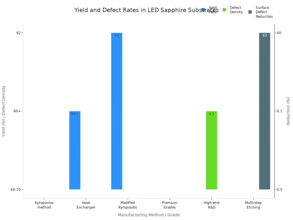
Yield and defect rate serve as primary indicators of production efficiency in LED sapphire substrate manufacturing. High yield means more usable substrates per batch, while a low defect rate ensures better product quality. Manufacturers often compare different crystal growth methods to optimize these metrics. For example, the Kyropoulos method typically achieves a yield rate between 60% and 70%. The heat exchanger method, popular in Japan and South Korea, can push yields above 80%. Some advanced Chinese manufacturers report yields up to 92% using modified Kyropoulos techniques. Defect density also varies, with premium grades targeting below 0.5 defects per square centimeter. High-end research and development lines can achieve even lower rates, sometimes below 0.1 defects per square centimeter.
| Parameter | Value / Range | Notes / Source Details |
|---|---|---|
| Yield Rate (Kyropoulos method) | 60-70% | Typical yield for KY method, widely used in China |
| Yield Rate (Heat Exchanger Method) | Above 80% | Used by Japanese and South Korean manufacturers |
| Modified Kyropoulos Yield | Up to 92% | Reported by emerging Chinese manufacturers |
| Defect Density (Premium Grades) | Below 0.5 defects/cm² | Target for premium sapphire substrates |
| Defect Density (High-end R&D) | Below 0.1 defects/cm² | Achieved by advanced inspection techniques |
| Surface Defect Reduction | Up to 40% reduction | Achieved via multi-step dry etching and AI-driven inspection |
Cycle Time and Throughput
Cycle time measures how long each production step takes, directly affecting throughput. In LED sapphire substrate production, dry etching typically requires 30 to 60 minutes per 2-inch wafer. The etch rate ranges from 50 to 200 nanometers per minute. Metrology steps, such as atomic force microscopy (AFM), take several minutes per measurement site, while 3D optical microscopy can complete measurements in just a few seconds. Faster measurement and etching processes allow manufacturers to increase throughput and reduce bottlenecks.
| Process Step | Description | Time Range / Rate |
|---|---|---|
| Dry Etching | Anisotropic etching of sapphire substrate using fluoride-based plasma and microwave energy. | 30 to 60 minutes per 2-inch wafer |
| Etch Rate | Speed of material removal during dry etching. | 50 to 200 nanometers per minute |
| Atomic Force Microscopy (AFM) | Measures PSS structures at discrete sites. | Several minutes per site |
| 3D Optical Microscopy | Uses white light interferometry for 3D surface measurement. | A few seconds per site |
Energy Consumption and Cost
Energy consumption and cost remain critical for manufacturers seeking competitive advantage. Efficient graphite mold design reduces the energy required for heating and cooling cycles. Lower defect rates and higher yields minimize wasted materials and rework, which further cuts costs. By optimizing cycle times and throughput, companies can produce more substrates with the same resources, improving overall profitability. Careful attention to these metrics ensures sustainable and cost-effective LED sapphire substrate production.
Graphite Mold Design Factors Affecting Production Efficiency

Graphite Mold Material Properties
The choice of graphite mold material plays a decisive role in the efficiency and quality of LED sapphire substrate production. Manufacturers prioritize several critical properties when selecting graphite materials:
- High thermal conductivity in graphite-like materials, such as graphene and reduced graphene oxide (rGO), enhances heat spreading and reduces thermal boundary resistance at the GaN/sapphire interface. This improvement leads to better LED performance and longer device life.
- Sapphire substrates have relatively poor thermal conductivity, which limits heat dissipation. Embedding a thin rGO layer between GaN and sapphire acts as a heat spreader, improving lateral heat flow.
- The rGO buffer layer can reduce thermal boundary resistance by about an order of magnitude, facilitating more efficient heat transfer.
- Improved GaN crystal quality on rGO buffers further enhances thermal management by reducing defects and non-radiative recombination.
- Graphite-based buffer layers support epitaxial lateral overgrowth of high-quality GaN, maintaining superior electrical and optical properties while improving heat dissipation.
Graphite purity, density, and grain size also influence mold performance. A purity level of 99.9% or higher ensures chemical stability, which is essential for producing high-quality substrates. Density values between 1.65 and 1.95 g/cm³ affect the mechanical strength and thermal properties of the graphite mold, impacting both durability and heat transfer efficiency. Grain size, ranging from 0.045 to 4 mm, determines machinability, surface finish, and mechanical strength. Fine porosity and a dense structure contribute to excellent strength and smooth surfaces, while low thermal expansion and high thermal conductivity reduce the risk of cracking and improve heat distribution. These factors allow companies like Ningbo VET Energy Technology Co., Ltd to customize graphite molds for specific industrial requirements, ensuring optimal substrate quality and production efficiency.
Graphite Mold Geometry and Precision
The geometry and precision of a graphite mold directly affect the dimensional accuracy and consistency of LED sapphire substrates. Precise mold geometry ensures uniform crystal growth and minimizes the risk of defects such as warping or uneven thickness. Manufacturers use advanced machining techniques to achieve tight tolerances and complex shapes, which are necessary for producing substrates that meet strict industry standards.
A well-designed graphite mold with accurate dimensions supports repeatable production cycles and reduces the need for post-processing. This precision leads to higher yields and lower defect rates. Companies like Ningbo VET Energy Technology Co., Ltd invest in state-of-the-art equipment to maintain high levels of mold accuracy, which translates into better substrate quality and improved manufacturing efficiency.
Graphite Mold Surface Finish and Coating
Surface finish and coating choices for graphite molds play a crucial role in substrate release, defect rates, and mold lifespan.
- Mold release agents, including graphite-based types, act as lubricants or barriers to prevent adhesion between the mold and substrate, making substrate release easier.
- Non-permanent and semi-permanent release agents exist; semi-permanent coatings form durable layers that improve surface quality and consistency, reducing defect rates.
- Proper selection of release agents enhances productivity, reduces defects, and extends mold life by minimizing sticking and wear.
- Compatibility with operating temperature and chemical environment is essential to prevent failure of release agents, which could otherwise increase defects or shorten mold lifespan.
- Graphite is a common mold release material, facilitating substrate release and potentially improving both defect rates and mold longevity.
- Mold releases improve surface quality and reduce defects by preventing material adhesion and enabling clean separation.
Coatings such as diamond-like carbon (DLC) can further improve hardness and wear resistance. Surface pretreatment, like plasma nitriding and repolishing, enhances coating adhesion and wear behavior. These measures help maintain mold performance and extend service life, which is vital for high-volume LED sapphire substrate production.
Graphite Mold Thermal Management Features
Thermal management features in graphite mold design are essential for maintaining process stability and substrate quality. High thermal conductivity in the mold material ensures rapid and uniform heat distribution during crystal growth and cooling cycles. This property minimizes thermal gradients, which can cause stress and defects in the sapphire substrate.
Engineers often incorporate features such as optimized cooling channels or heat sinks into the graphite mold design. These additions help control temperature fluctuations and improve overall process efficiency. By managing heat flow effectively, manufacturers reduce cycle times and energy consumption, leading to cost savings and higher throughput. Ningbo VET Energy Technology Co., Ltd leverages advanced thermal management strategies in their graphite mold solutions, supporting customers in achieving consistent, high-quality LED sapphire substrates.
Manufacturers achieve high efficiency in LED sapphire substrate production by focusing on graphite mold design.
- Material properties, geometry, surface finish, and thermal management each play a vital role.
- Continuous innovation in graphite mold technology helps companies improve yield, reduce costs, and maintain a competitive edge.
FAQ
What is the main benefit of using high-purity graphite in mold design?
High-purity graphite improves chemical stability. Manufacturers achieve better substrate quality and reduce contamination risks during LED sapphire substrate production.
How does mold geometry affect LED sapphire substrate yield?
Precise mold geometry ensures uniform crystal growth. Manufacturers see fewer defects and higher yields when molds maintain tight dimensional tolerances.
Can surface coatings extend graphite mold lifespan?
Yes. Surface coatings like diamond-like carbon increase hardness and wear resistance. These coatings help molds last longer and maintain consistent performance.

