
Epi Graphite Barrel Susceptor


Epitaxial Epi Graphite Barrel Susceptor
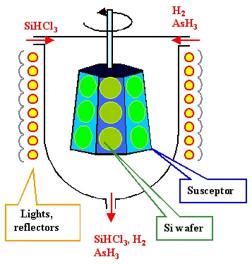
Epitaxial Epi Graphite Barrel Susceptor is a specially designed support and heating device used to hold and heat semiconductor substrates during manufacturing processes like Deposition or Epitaxy processes.

Its structure includes typically cylindrical or slightly barrel-shaped, surface features multiple pockets or platforms for placing the wafers, can be solid or hollow design, depending on the heating method.


The main functions of epitaxial barrel susceptor:

1. Wafer Carrier and Temperature Control

The susceptor surface is designed with multiple wafer pockets (such as hexagonal or octagonal arrangement), which can support 6-15 wafers simultaneously. The high thermal conductivity of high-purity graphite (120-150W/m.K) ensures rapid heat transfer, combined with rotation function (5-20 RPM), resulting in a wafer surface temperature deviation of<± 1 ℃ and epitaxial layer thickness uniformity of<1%.


2. Optimization of reactant gas flow direction
The microstructure of the susceptor surface can break the boundary layer effect, allowing for uniform distribution of reaction gases (such as SiH4, NH3) and improving the consistency of deposition rate.

3. Anti pollution and anti-corrosion protection
Graphite substrates are prone to decomposition and release metal impurities (such as Fe,Ni) at high temperatures, while a 100μm thick CVD SiC coating can form a dense barrier to suppress graphite volatilization, resulting in a wafer defect rate of<0.1 defects/cm ².
Applications:

  1. Primarily used for silicon epitaxial growth.
  2. Also suitable for epitaxy of other semiconductor materials like GaAs, InP, etc.

VET Energy utilizes high-purity graphite with CVD-SiC coating to enhance chemical stability:

   1. High-Purity Graphite Material

       High Thermal Conductivity: Graphite’s thermal conductivity is three times that of silicon, enabling rapid heat transfer from the source to the wafer, reducing heating time.
       Mechanical Strength: Isostatic pressure graphite density ≥ 1.85 g/cm³, capable of withstanding temperatures above 1200℃ without deformation.
   2. CVD-SiC Coating

        A β-SiC layer is formed on the graphite surface via chemical vapor deposition (CVD), with a purity of ≥ 99.99995%.
       Coating thickness uniformity error is less than ±5%, and surface roughness is below Ra0.5μm.
  3. Performance Enhancements

      Corrosion Resistance: Withstands highly corrosive gases like Cl2 and HCl, extending GaN epitaxy lifespan by three times in NH3 environments.
      Thermal Stability: Coefficient of thermal expansion (4.5 × 10⁻⁶/℃) matches graphite, preventing coating cracks from temperature fluctuations.
      Hardness and Wear Resistance: Vickers hardness reaches 28 GPa, 10 times higher than graphite, reducing wafer scratch risks.


More Posts

C/C Composites vs. Metal Bipolar Plates: Which Material Is Winning the Thermal Management Race?

As the global push for hydrogen energy accelerates, fuel cell technology is moving from laboratory breakthroughs to large-scale commercial deployment. At the heart of this transition is the bipolar plate (BPP)—a critical component accounting for up to 70% of a fuel cell stack’s weight and a significant portion of its cost.

While bipolar plates are responsible for distributing reactants and conducting electricity, their most unforgiving job is thermal management. Fuel cells generate massive amounts of waste heat; if a plate cannot dissipate or regulate this heat efficiently, the stack suffers from localized hot spots, membrane degradation, and a drastically shortened lifespan.

Today, a fierce material science race is underway between Carbon/Carbon (C/C) Composites and Metal Bipolar Plates. Which one is truly winning the thermal management race? Let’s break down the data.

From Atomic Interfaces to Wafer Yield: What van der Waals Epitaxy Teaches Us About Semiconductor Coating Engineering

At the heart of semiconductor epitaxy lies a fundamental pursuit: growing high-quality crystalline materials on foreign substrates. The enduring challenge of conventional heteroepitaxy is lattice mismatch—when two materials have different interatomic spacings, misfit dislocations and defects proliferate at the interface, severely compromising device performance. This physical constraint is precisely the same dilemma facing CVD coatings on graphite susceptors: Coefficient of Thermal Expansion (CTE) mismatch between coating and substrate induces interfacial stress accumulation, micro-crack initiation, and ultimately coating delamination and wafer contamination.

In recent years, groundbreaking advances in “van der Waals epitaxy” have offered a transformative perspective for understanding and engineering coating-substrate interfaces.

Microstructure Dictates Macro Yield: Grain Boundary Engineering in Advanced CVD Coatings and the Path to Semiconductor “Zero-Defect” Manufacturing

In the grand narrative of semiconductor manufacturing, we habitually speak of wafer dimensions, node precision, and process temperatures. Yet, as the industry resolutely marches toward the “zero-defect” goal, the battle is often won or lost at a far smaller scale—within those coatings, only a few hundred microns thick, that protect critical components. The macroscopic performance of a material is ultimately dictated by its microstructure: grain size, grain boundary density, and crystallographic texture. For critical consumables like graphite susceptors that endure extreme thermo-chemical shocks, the “microstructure engineering” of advanced CVD coatings is emerging as the invisible fulcrum for breaking through yield bottlenecks.

Send Us A Message

Looking forward to your contact with us

Let's have a chat

🇺🇸 English
🇺🇸 English
🇸🇦 Arabic
🇵🇹 Portuguese
🇷🇺 Russian
🇪🇸 Spanish