
The Vulnerability of Traditional Graphite In MOCVD and SiC epitaxy, hydrogen is frequently used as a carrier gas. At high temperatures, hydrogen becomes highly aggressive, leading to the erosion of standard SiC coatings and the subsequent “dusting” of the underlying graphite. This contamination is the silent killer of wafer yield.
The Vetek Advantage: Engineered Resilience At Vetek Semiconductor, our TaC coating technology is specifically engineered to act as an impenetrable barrier in these “harsh chemistry” environments:
Superior Chemical Stability: Unlike standard coatings, our TaC layers are virtually inert to hydrogen and ammonia even at 2200°C, ensuring zero carbon inclusion and consistent wafer purity.
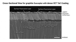
Thermal Shock Resistance: We utilize a proprietary CVD process that ensures a high-strength bond between the TaC layer and the isostatic graphite substrate, preventing delamination during rapid ramp-up and ramp-down cycles.
Extended Consumable Life: By eliminating chemical erosion, our TaC-coated susceptors and components offer a significantly longer service life, directly reducing the Total Cost of Ownership (TCO) for our clients.
Meeting the 2026 Power Demand From high-voltage MOSFETs to next-generation GaN-on-SiC devices, the reliability of the substrate is non-negotiable. Our goal at Vetek is to provide the “Material Foundation” that allows engineers to focus on device performance without worrying about chamber contamination.
Consultative Engineering Every reactor is different. We don’t just supply parts; we collaborate on custom designs and coating thicknesses to optimize the flow dynamics and thermal profiles of your specific system.
Request a Technical Consultation: Interested in benchmarking our TaC coatings against your current solution? Contact us for comparative wear-test data and SEM analysis.

 French
  English
  Japanese
  German
  Korean
  Arabic
  Portuguese
  Danish
  Spanish
  Finnish
  Indonesian
  Italian
  Russian
  Persian