
High Strength Glass Carbon Crucible For High-temperature Synthesis

Heat Resistant Glass Carbon Crucible are specialized crucibles designed for high-temperature experiments and applications. They offer excellent heat resistance, chemical stability, and high purity, making them widely used in industries like metallurgy, ceramics, chemicals, and semiconductors.
Their production involves a complex process, including using high-purity materials like graphite and asphalt, undergoing high-temperature treatments, forming, sintering, annealing, grinding, and polishing to ensure top quality and performance.

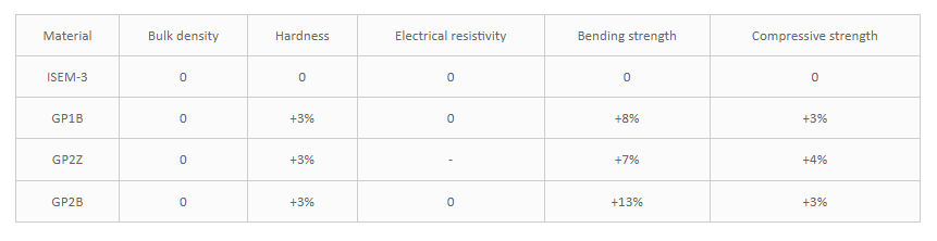
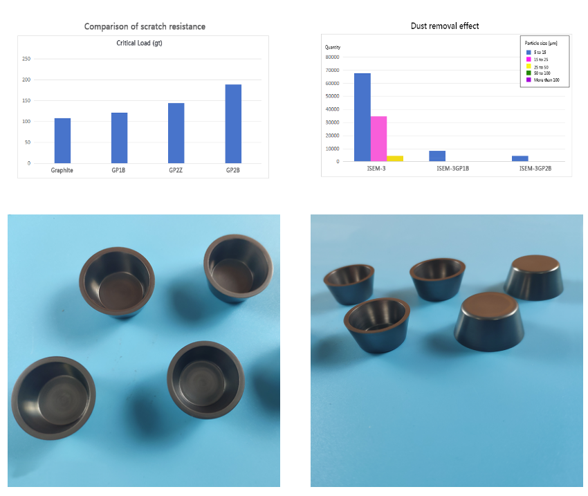
Heat Resistant Glass Carbon Crucible features include compatibility with various graphite materials as substrates, maintaining the graphite substrate’s properties, reducing graphite dust formation, and offering improved scratch resistance and enhanced anti-friction durability.

We supply components for monocrystalline silicon drawing equipment, epitaxial growing parts, continuous casting dies, and glass seal fixtures. Let us know if you need more details!
 

Membagikan:

Lebih banyak posting

Beyond Silicon: Why TaC Coating is Becoming the Gold Standard for 2000°C+ Environments

In the rapidly evolving power electronics landscape of 2026, we are pushing wide-bandgap semiconductors to their physical limits. As the demand for higher growth rates and superior crystalline quality intensifies, the industry is moving toward higher processing temperatures—often exceeding 2000°C. At these extremes, traditional materials fail, and Tantalum Carbide (TaC) coating emerges as the critical enabler.

Scaling Excellence: Solving Thermal Field Challenges in the 8-Inch SiC Era

In 2026, the semiconductor industry is no longer just a race for smaller nanometers; it is a race for material stability at extreme limits. As global production scales toward 8-inch Silicon Carbide (SiC) wafers to meet the demands of AI and high-voltage power electronics, the industry faces a critical bottleneck: Thermal Field Uniformity.

Navigating the 200mm Transition: Why TaC Coating is the Deciding Factor for 8-inch SiC Yields

Introduction As the global power electronics industry aggressively shifts from 150mm (6-inch) to 200mm (8-inch) SiC wafer production, the conversation often stays on the reactors themselves. However, at the heart of the MOCVD and Epitaxy process lies a silent but critical component: the graphite susceptor. If you are seeing a drop in yield or unexpected crystal defects as you scale to 8-inch, you aren’t alone. The thermal and chemical stresses at 1600°C+ are pushing traditional coatings to their breaking point.

The Endgame of 200mm SiC Scaling: Who Defines the Yield Ceiling in 2026?

As global leaders transition to total 200mm (8-inch) SiC production, the industry focus has shifted from “capacity” to “atomic-level control.” In the high-stakes environment of 2026, the real competition isn’t about wafer count—it’s about the coating technology that dictates your Fab’s bottom line.

Kirimi kami pesan

id_IDIndonesian

Menantikan kontak Anda dengan kami

Ayo ngobrol

