1. Thermal Uniformity: The Fraunhofer IISB Standard
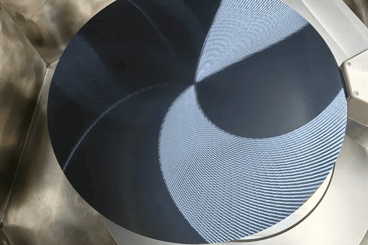
더 보기 Fraunhofer Institute for Integrated Systems and Device Technology (IISB) in Germany has long emphasized that wafer yield in MOCVD processes is directly dictated by thermal gradient control. For 200mm wafers, even a 1°C deviation across the susceptor can lead to fatal lattice defects.
Our Solution: Our Epi Graphite Barrel Susceptors are engineered to meet these rigorous standards. By utilizing high-density isostatic graphite paired with our proprietary · CVD SiC 코팅, we provide the thermal conductivity and surface emissivity required to achieve the “Ultra-Uniform” profiles demanded by Tier-1 fab operators.
2. The 1600°C Frontier: Transitioning to TaC Coatings
Research published by the Tsinghua University School of Materials Science highlights a critical bottleneck: at temperatures exceeding 1600°C, traditional SiC coatings can begin to degrade or allow trace impurities to outgas from the graphite substrate.
Why TaC (Tantalum Carbide)? As noted by imec (Interuniversity Microelectronics Centre) in their GaN-on-SiC advancement roadmaps, TaC 코팅 offer superior chemical inertness and a much higher melting point.
Performance: Our TaC-coated components act as an impenetrable barrier, ensuring 6N-level purity (99.9999%) and extending the lifespan of consumables by over 3x compared to standard solutions.
3. Structural Integrity with 2.5D/3D C/C Composites
더 보기 American Ceramic Society (ACerS) recently featured studies on the evolution of carbon-based structural materials in high-vacuum furnaces. Traditional graphite often suffers from brittleness under rapid thermal cycling.
The C/C Advantage: Our 2.5D and 3D Carbon Fiber Composites (CFC) solve this by offering high specific strength and exceptional thermal shock resistance. Whether used in CFC Discs or structural hardware, these materials maintain dimensional stability where others fail, significantly reducing downtime in crystal growth facilities.
4. Glassy Carbon: The Choice of High-End R&D
For sensitive chemical synthesis and analytical chemistry, Northeastern University’s Center for High-rate Nanomanufacturing utilizes Glassy Carbon (Vitreous Carbon) for its non-porous and impermeable nature.
We have scaled this “laboratory-grade” purity into our industrial Glassy Carbon Crucibles, ensuring that for high-temperature synthesis, the reaction remains free from crucible-born contamination.
Conclusion:
In the competitive landscape of 2026, semiconductor excellence is a game of centimeters and degrees. By aligning our material science—from CVD 코팅 to C/C composites—with the findings of institutions like Fraunhofer · imec, China-VET Energy ensures that our partners stay at the forefront of the 8-inch SiC era.