
Что такое покрытие SIC?
Покрытие CVD SiC относится к карбиду кремния, полученному методом химического осаждения из паровой фазы — вакуумного процесса для материалов высокой чистоты. Он обладает превосходными термическими, электрическими и химическими свойствами, что делает его идеальным для полупроводниковых применений, таких как травление, MOCVD, эпитаксиальное Si, эпитаксиальное SiC и оборудование для быстрой термической обработки. Этот метод обеспечивает высокую однородность, чистоту и контроль процесса.
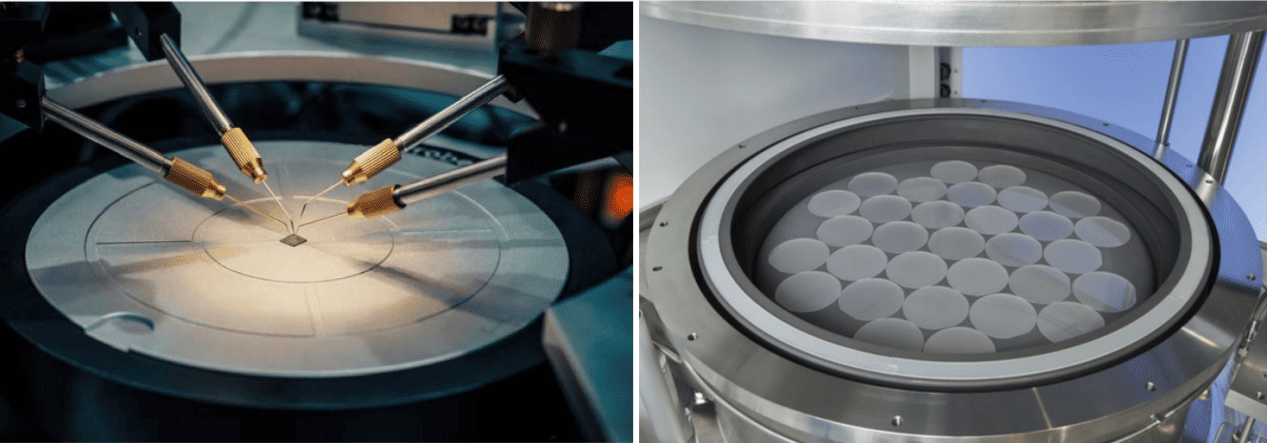
Температура поверхности графитовой подложки существенно влияет на процесс нанесения покрытия CVD-SiC. При высоких температурах промежуточные газы десорбируются и выделяются, оставляя C и Si, образуя твердофазные покрытия SiC. Чтобы изучить, как температура осаждения влияет на микроскопическую морфологию и плотность покрытия, эксперименты проводились при 900℃, 1000℃, 1100℃, 1200℃ и 1300℃. Результаты показаны в таблице 3 и на рисунке 2.
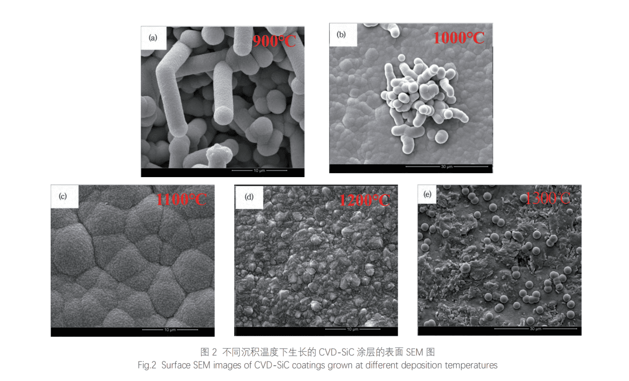
Когда температура осаждения достигает 900 ℃, весь SiC превращается в волокна. Видно, что диаметр одного волокна составляет около 3,5 мкм, а его соотношение сторон составляет около 3 (<10). Более того, он состоит из бесчисленного количества частиц нано-SiC, поэтому принадлежит к поликристаллической структуре SiC, которая отличается от традиционных нанопроволок SiC и монокристаллических усов SiC. Этот волокнистый SiC является структурным дефектом, вызванным необоснованными параметрами процесса. Видно, что структура этого покрытия SiC относительно рыхлая, между волокнистым SiC имеется большое количество пор, а плотность очень низкая. Следовательно, эта температура не подходит для получения плотных покрытий SiC. Обычно дефекты структуры волокнистого SiC возникают из-за слишком низкой температуры осаждения. При низких температурах малые молекулы, адсорбированные на поверхности подложки, обладают низкой энергией и плохой миграционной способностью. Следовательно, небольшие молекулы имеют тенденцию мигрировать и расти до самой низкой поверхностной свободной энергии зерен SiC (например, кончика зерна). Непрерывный направленный рост в конечном итоге приводит к образованию волокнистых структурных дефектов SiC.
Подготовка покрытия CVD SiC:
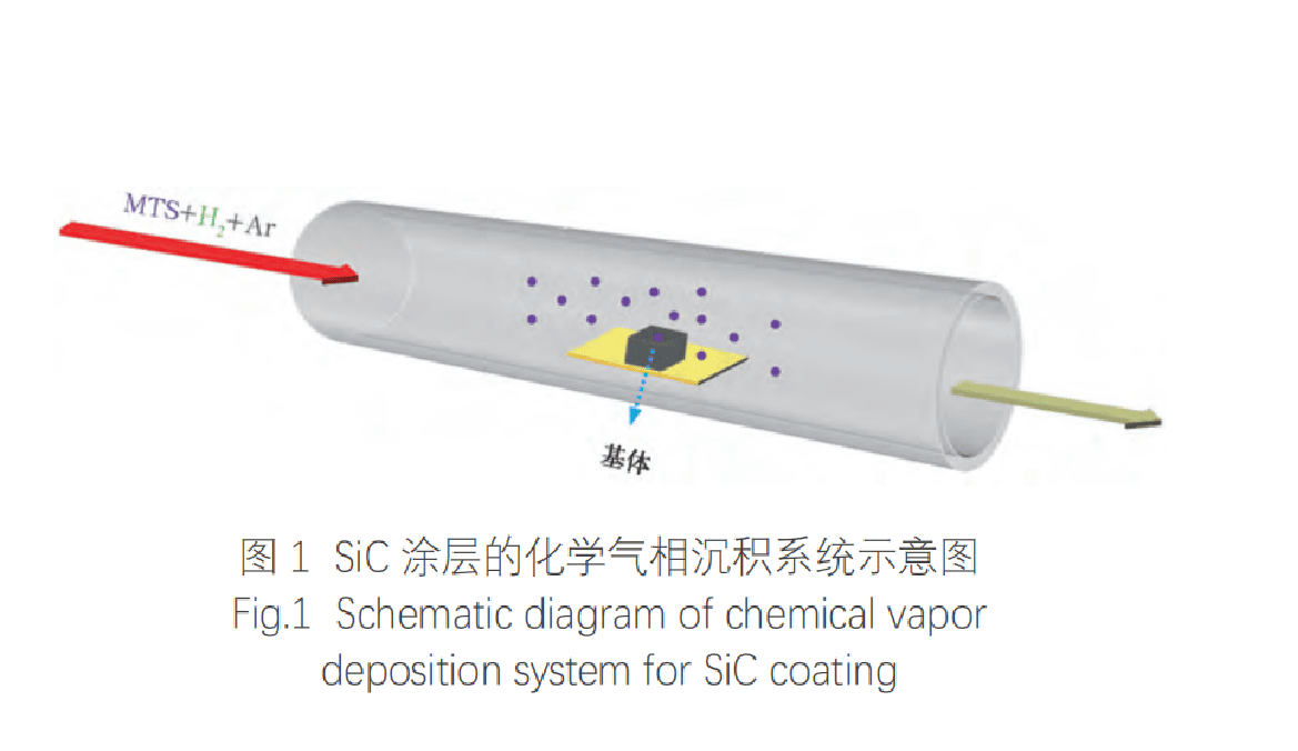
Сначала графитовую подложку помещают в высокотемпературную вакуумную печь и выдерживают при температуре 1500 ℃ в течение 1 часа в атмосфере Ar для удаления золы. Затем графитовый блок разрезается на блок размером 15х15х5мм и поверхность графитового блока шлифуется наждачной бумагой размером 1200 меш для устранения поверхностных пор, которые влияют на осаждение SiC. Обработанный графитовый блок промывают безводным этанолом и дистиллированной водой, а затем помещают в печь при температуре 100 ℃ для сушки. Наконец, графитовую подложку помещают в основную температурную зону трубчатой печи для осаждения SiC. Принципиальная схема системы химического осаждения из паровой фазы показана на рисунке 1.
Покрытие CVD SiC было исследовано с помощью сканирующей электронной микроскопии для анализа размера и плотности его частиц. Скорость осаждения рассчитывали по формуле:
VSiC = (m₂ – m₁) / (S × t) × 100%
где VSiC — скорость осаждения, m₂ — масса образца с покрытием (мг), m₁ — масса подложки (мг), S — площадь поверхности подложки (мм²), а t — время осаждения (ч).
Процесс CVD-SiC включает термическое разложение MTS при высоких температурах, в результате чего образуются небольшие молекулы источника углерода (такие как CH₃, C2H₂ и C2H₄) и молекулы источника кремния (такие как SiCl₂ и SiCl₃). Эти молекулы переносятся к поверхности графитовой подложки газами-носителями и разбавителями, где они адсорбируются и вступают в реакцию с образованием капель, которые постепенно растут и сливаются. В ходе реакции также образуются побочные продукты, такие как газообразный HCl.
При 1000 °C плотность покрытия SiC значительно увеличивается. Покрытие состоит в основном из зерен SiC размером около 4 мкм, но некоторые волокнистые дефекты SiC указывают на направленный рост и недостаточное уплотнение.
При 1100 °С покрытие становится очень плотным, без волокнистых дефектов. Он состоит из частиц SiC каплевидной формы (диаметром 5–10 мкм), состоящих из многочисленных наноразмерных зерен SiC. Под контролем массопереноса адсорбированные молекулы обладают достаточной энергией и временем для зарождения и формирования сферических капель, которые плотно объединяются в плотное покрытие.
При 1200 °С покрытие остается плотным, но морфология становится многоребристой, а поверхность более шероховатой.
При 1300 °C происходит зарождение газовой фазы из-за быстрого разложения МТС. SiC зарождается до того, как достигает подложки, образуя правильные сферические частицы (~ 3 мкм), которые осаждаются рыхло, что приводит к образованию покрытия с низкой плотностью. Эта температура непригодна для плотного покрытия SiC.
Таким образом, 1100 °C является оптимальной температурой осаждения для получения плотных покрытий CVD-SiC.
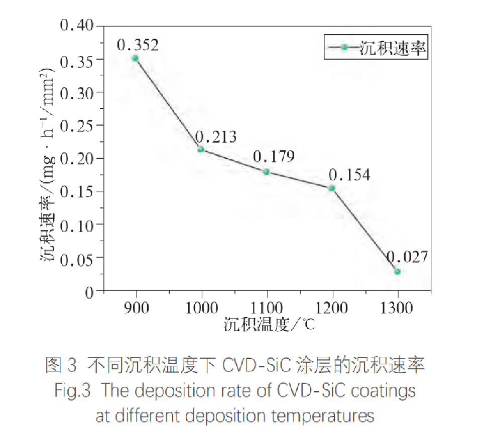
На рис. 3 показана скорость осаждения CVD-покрытий SiC при различных температурах осаждения. С увеличением температуры осаждения скорость осаждения покрытия SiC постепенно снижается. Скорость осаждения при 900°C составляет 0,352 мг·ч-1/мм2, а направленный рост волокон приводит к наибольшей скорости осаждения. Скорость осаждения покрытия с наибольшей плотностью составляет 0,179 мг·ч-1/мм2. Из-за осаждения некоторого количества частиц SiC скорость осаждения при 1300°С самая низкая, всего 0,027 мг·ч-1/мм2. Вывод: Лучшая температура CVD-осаждения составляет 1100 ℃. Низкая температура способствует направленному росту SiC, тогда как высокая температура вызывает осаждение SiC из паровой фазы и приводит к образованию разреженного покрытия. С повышением температуры осаждения скорость осаждения CVD-покрытие SiC постепенно снижается.