
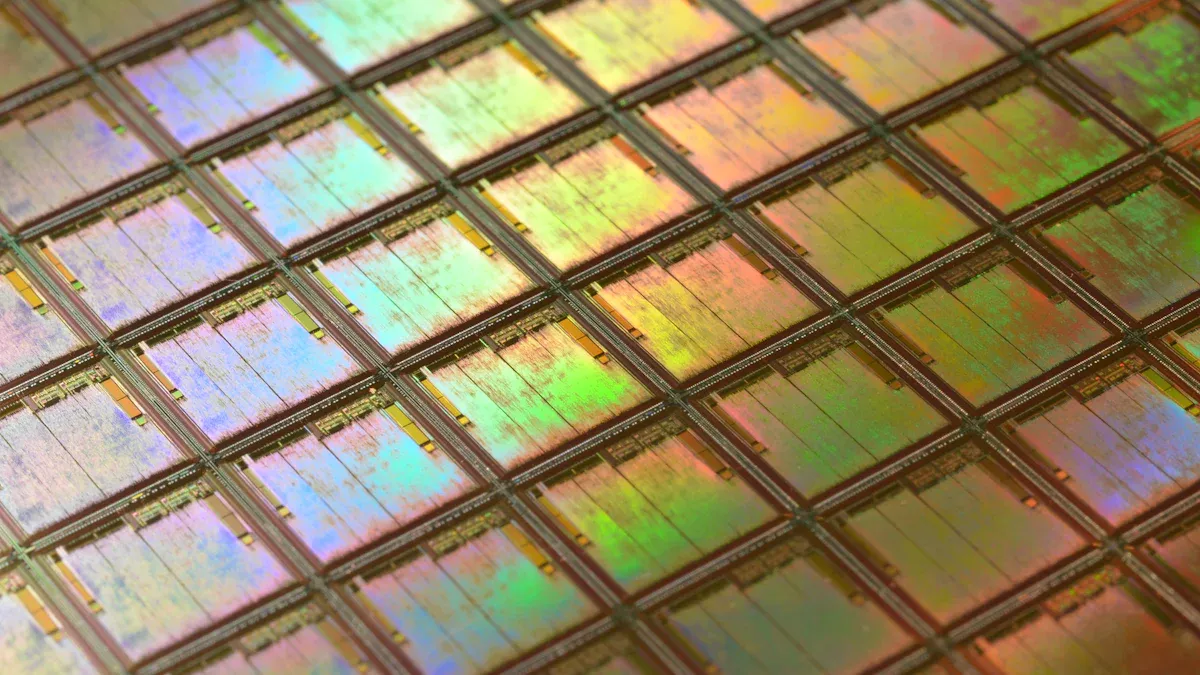
Semiconductor graphite plays a crucial role in wafer production. Its unique properties, such as high thermal conductivity and chemical stability, make it indispensable in the semiconductor process. For instance, specialty graphite ensures precise temperature control and uniform heat distribution during wafer processing. Its ability to endure harsh conditions, like chemical etching, further enhances its reliability. The rise in advanced semiconductor technologies has also increased the demand for materials like porous graphite, which supports high-performance manufacturing. Additionally, coatings such as tac coating on graphite and sic coating on graphite improve durability and efficiency, making semiconductor graphite a cornerstone of innovation.
Key Takeaways
- Semiconductor graphite is important for making wafers. It spreads heat evenly and lowers defects in the product.
- It is chemically stable, so it handles tough conditions well. This makes parts last longer and need less fixing.
- Using semiconductor graphite improves accuracy and quality. It is eco-friendly and meets the need for better semiconductor devices.
Unique Properties of Semiconductor Graphite
High Thermal Conductivity
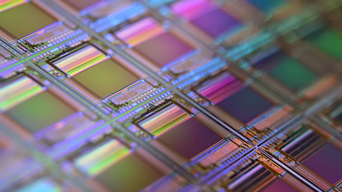
Semiconductor graphite excels in thermal conductivity, making it a critical material in wafer production. Its ability to transfer heat efficiently ensures uniform temperature distribution during high-temperature processes like wafer growth. This property minimizes thermal stress, reducing the risk of defects in the final product.
📌 Did you know? Semiconductor graphite is increasingly used in advanced semiconductor devices due to its excellent electrical and thermal properties. As the demand for smaller, more efficient devices grows, its role becomes even more vital.
Additionally, its high thermal conductivity supports energy efficiency, which is essential for sustainable manufacturing. This makes it a preferred choice for industries aiming to optimize performance while reducing environmental impact.
Chemical Stability in Extreme Conditions
The chemical stability of semiconductor graphite allows it to withstand harsh environments without degrading. It resists corrosion and maintains its integrity even when exposed to reactive chemicals during etching and deposition processes. This reliability ensures consistent performance, which is crucial for producing high-quality wafers.
- Key Benefits of Chemical Stability:
- Prolonged lifespan of components.
- Reduced maintenance and replacement costs.
- Enhanced precision in semiconductor manufacturing.
This stability makes semiconductor graphite indispensable in processes requiring high precision and durability.
Mechanical Strength and Durability
Semiconductor graphite demonstrates exceptional mechanical strength, enabling it to handle the delicate yet demanding nature of wafer production. Graphite wafer carriers, for example, provide excellent thermal stability and mechanical resilience, ensuring safe handling of wafers during processing.
- Durability Highlights:
- Components like Mersen’s carriers endure harsh conditions, extending their lifespan.
- Reduced replacement frequency leads to significant cost savings.
- Consistent performance supports high-precision manufacturing.
The combination of strength and durability not only enhances operational efficiency but also contributes to long-term cost-effectiveness. This makes semiconductor graphite a sustainable and reliable choice for the semiconductor industry.
Role of Semiconductor Graphite in Wafer Production
High-Temperature Applications in Wafer Growth
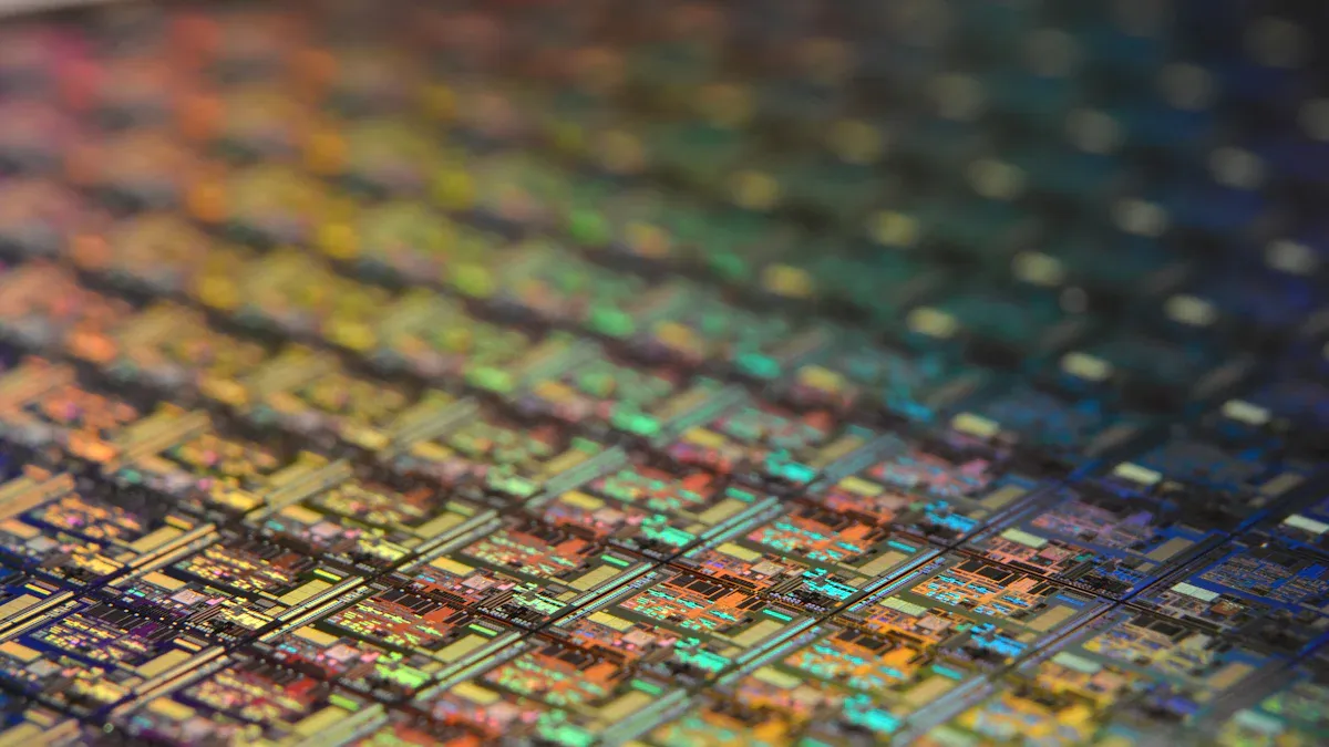
Semiconductor graphite plays a critical role in wafer growth processes that require extreme heat. You can rely on its thermal stability and low expansion coefficients to maintain precision during high-temperature operations. These properties ensure that dimensional changes are minimal, which is essential for producing high-quality wafers.
| Evidence Type | Description |
|---|---|
| Thermal Stability | Maintains performance under extreme heat conditions. |
| Low Expansion Coefficients | Reduces dimensional changes during wafer growth. |
| Excellent Thermal Conductivity | Provides precise temperature control for consistent results. |
| Durability Under Extreme Conditions | Extends the lifespan of components used in wafer production. |
The ability of semiconductor graphite to sustain high temperatures without losing integrity makes it indispensable in modern semiconductor manufacturing. This ensures that you achieve both efficiency and precision in wafer production.
Use in Crucibles, Heaters, and Molds
Graphite’s unique properties make it ideal for fabricating crucibles, heaters, and molds used in wafer production. Its high thermal conductivity ensures even heat distribution, while its chemical inertness prevents contamination during processing. These characteristics allow you to achieve consistent results in every production cycle.
- Key advantages of semiconductor graphite in these applications:
- High thermal conductivity for uniform heating.
- Chemical inertness to maintain purity.
- Thermal stability for reliable performance.
By using semiconductor graphite in these components, you can enhance the efficiency and quality of your manufacturing processes. This material ensures that your equipment operates at peak performance, even under demanding conditions.
Precision and Quality in Etching and Deposition Processes
Semiconductor graphite ensures precision and quality during etching and deposition processes. Its chemical stability allows it to resist corrosion from reactive chemicals, ensuring consistent performance. This reliability helps you produce wafers with intricate designs and high accuracy.
The semiconductor industry continues to grow, driven by advancements in consumer electronics, automotive, and telecommunications. Graphite wafer carriers, known for their thermal stability and mechanical strength, support this growth by enabling delicate wafer handling during these critical processes.
- Benefits of using semiconductor graphite:
- Enhanced precision in etching intricate patterns.
- Consistent quality in deposition layers.
- Reduced risk of defects in the final product.
By incorporating semiconductor graphite into your production line, you can meet the increasing demand for smaller, more efficient semiconductor devices.
Advantages of Semiconductor Graphite Over Other Materials
Comparison with Metals in Thermal and Electrical Conductivity
When comparing semiconductor graphite to metals, you’ll notice its superior thermal and electrical properties. Metals like copper and aluminum conduct electricity well, but they often struggle with thermal stability at high temperatures. Semiconductor graphite, on the other hand, maintains its performance even in extreme heat. This makes it ideal for applications like wafer growth, where precise temperature control is critical.
Additionally, graphite’s lightweight nature gives it an edge over metals. You can achieve the same or better thermal conductivity without adding unnecessary weight to your equipment. This not only improves efficiency but also reduces wear and tear on machinery.
Benefits Over Ceramics in Durability and Cost
Ceramics are known for their heat resistance, but they lack the mechanical strength and flexibility of semiconductor graphite. When subjected to stress, ceramics can crack or break, leading to costly replacements. Graphite, however, offers exceptional durability. It withstands mechanical stress and maintains its structure over time.
From a cost perspective, graphite proves to be more economical. While ceramics may have a lower initial cost, their frequent replacements and maintenance expenses add up. By choosing semiconductor graphite, you invest in a material that lasts longer and performs consistently, saving you money in the long run.
Long-Term Cost-Effectiveness and Sustainability
Semiconductor graphite stands out as a sustainable choice for wafer production. Its long lifespan reduces the need for frequent replacements, minimizing waste. You also benefit from its energy efficiency, as its high thermal conductivity lowers energy consumption during manufacturing processes.
Moreover, graphite’s recyclability adds to its sustainability. You can repurpose used graphite components, reducing environmental impact. By integrating semiconductor graphite into your production line, you not only enhance efficiency but also contribute to a greener future.
Semiconductor graphite remains essential for wafer production due to its unmatched properties. Its thermal stability, chemical resistance, and mechanical strength ensure precision and efficiency in manufacturing. You can see its impact across applications like semiconductor wafers, electrodes, and heat sinks, as shown below:
| Application | Description |
|---|---|
| Semiconductor Wafers | Thin slices of semiconductor material, increasingly utilizing graphite for specialty applications. |
| Electrodes | Used in various electronic applications due to their conductive properties. |
| Heat Sinks | Effective in dissipating heat in semiconductor devices, enhancing performance. |
As the semiconductor industry evolves, semiconductor graphite will continue to drive innovation and production quality.
FAQ
What makes semiconductor graphite better than other materials for wafer production?
Semiconductor graphite offers unmatched thermal stability, chemical resistance, and mechanical strength. These properties ensure precision and efficiency in wafer production, making it superior to metals and ceramics.
How does Ningbo VET Energy Technology Co. contribute to semiconductor manufacturing?
Ningbo VET Energy Technology Co. provides high-quality semiconductor graphite solutions. Their products enhance wafer production by ensuring durability, precision, and sustainability in demanding manufacturing environments.
Can semiconductor graphite be recycled?
Yes, you can recycle semiconductor graphite. Its recyclability reduces waste and supports sustainable manufacturing, making it an environmentally friendly choice for the semiconductor industry.

