
Core Applications of TAC Coating in Semiconductor Manufacturing

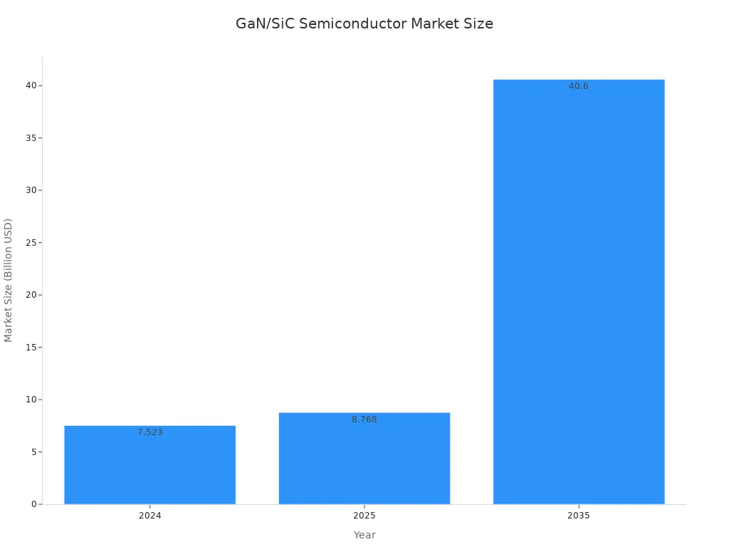
TaC coating is a high-performance ceramic layer critical to advanced semiconductor manufacturing, particularly suited for SiC single crystal growth and GaN/SiC epitaxial processes. The rapidly expanding GaN/SiC semiconductor market is projected to reach US$7.523 billion by 2024, growing at a compound annual growth rate of 16.56% between 2025 and 2035.
Tantalum carbide (TaC) is its primary chemical composition. Researchers study the Ta–C–N system, where TaC1-xNx represents the chemical composition. The base structure in experiments is the face-centered cubic (fcc) structure of Ta–C. Stable binary structures include fcc-TaC and hexagonal TaN (hex-TaN). For the cubic structure of Ta–C, non-metal vacancies are more critical than metal vacancies. Physical vapor deposition (PVD) can stabilize the fcc-structured Ta–C–N due to its highly constrained kinetics and the introduction of structural defects. In the TaC1-xNx system, a phase transition from single-phase fcc-Ta1-y-zCyNz to fcc + hexagonal Ta1-y-zCyNz occurs near x ≈ 0.68. Manufacturers prepare four different crystal structures of TaC coatings on carbon/carbon composites. These structures include an acicular crystal structure, which exhibits better ablation resistance.


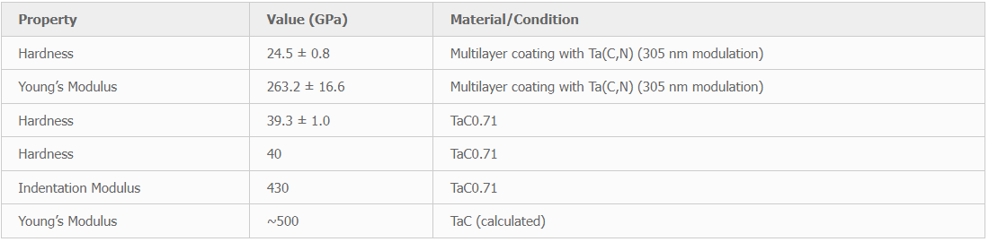
TaC coating is a specialized material that enhances computer chip performance, especially in high-temperature environments. It effectively prevents harmful substances from entering the chip, ensuring cleanliness and durability. Compared to other materials, TaC coating delivers superior performance, enabling higher-quality chip production and improved computer and smartphone functionality. Additionally, it exhibits exceptional mechanical properties, such as Ta(C,N) (305 nm modulation) multilayer coating with a hardness of 24.5 ± 0.8 GPa and Young’s modulus of 263.2 ± 16.6 GPa. TaC0.71 has a hardness of 39.3 ± 1.0 GPa, with some measurements reaching 40 GPa. Its indentation modulus is 430 GPa, while TaC’s calculated Young’s modulus is approximately 500 GPa.


The purity requirement for silicon carbide coatings exceeds 99.9995%, with the ability to withstand temperatures up to 1600°C. Its primary function is to isolate gaseous silicon and graphite, preventing reactions that generate silicon carbide particles and thereby avoiding wafer contamination. Given that silicon carbide constitutes a significant proportion of the cost in epitaxial crystal growth processes – accounting for over 40-50% of domestic crystal growth expenses – controlling the cost structure of silicon carbide crystal growth is paramount. Sustained material innovation and technological advancement are pivotal to overcoming industry challenges. Currently, graphite and silicon carbide ceramic materials are indispensable in semiconductor production, extensively utilised in critical components such as heaters, bases, crucibles, flow tubes, and connectors. The purity, chemical stability, and particularly the volatility of these materials directly impact the purity, performance, and quality of semiconductor materials.


Methods for preparing silicon carbide coatings include chemical vapour deposition (CVD), slurry pyrolysis, and plasma spraying. Among these, CVD technology is the most mature, yet it faces numerous technical limitations, high costs, and extended lead times.




More Posts

Pushing the Limits: The Engineering Challenge Behind Sub-1.2mm Graphite Bipolar Plates

In the race for higher fuel cell power density, every millimeter counts. And right now, the industry is fixated on a single number: 1.2mm.

Tracing the evolution of fuel cell stacks, graphite bipolar plate thickness has undergone a remarkable reduction—from approximately 2mm in early designs down to 1.5–1.66mm. As the industry demands ever-higher stack power density (now reaching 3.8–4.5 kW/L), compressing plate thickness below 1.2mm has become an inevitable choice for boosting volumetric power and reducing system weight.

But here’s the challenge: graphite is brittle. It’s porous. It’s naturally resistant to thinning. When plates drop below 1.2mm, the engineering obstacles multiply—gas permeability spikes, mechanical strength drops, and cracking during forming becomes a production nightmare.

This is the story of how the industry is overcoming those obstacles—and what it means for the future of fuel cell manufacturing.

From Bottleneck to Breakthrough: How Carbon Paper and GDL Localization Are Reshaping the Hydrogen Supply Chain

For years, the hydrogen fuel cell industry has been haunted by a single, thin, unassuming component: carbon paper. As the substrate for the gas diffusion layer (GDL), it’s smaller than a credit card and lighter than a feather, yet without it, a fuel cell simply cannot function.

And for most of the past decade, this critical material was the industry’s Achilles’ heel – expensive, unreliable in supply, and controlled by a handful of overseas suppliers. That bottleneck, however, is now cracking open.

2025–2026 marks a turning point. China’s carbon paper and GDL industry has moved from near‑total import dependence to full‑scale, world‑class production. The result is a global supply chain that is more diverse, more competitive, and more resilient – and that directly benefits every hydrogen player, from stack manufacturers to project developers, wherever they are based.

Pushing the Limits: The Engineering Challenge Behind Sub-1.2mm Graphite Bipolar Plates

Exploring the technological frontiers and industrialization pathways of ultra-thin graphite bipolar plates

As the hydrogen energy and energy storage industries move toward large-scale commercialization, stack power density and cost control have become central industry concerns. As one of the heaviest and most cost-intensive core components in a fuel cell stack, the thickness, electrical conductivity, and gas tightness of bipolar plates directly determine the performance ceiling of the entire system. When graphite bipolar plate thickness breaks through the 1.2mm threshold, we are no longer simply dealing with material thinning—this becomes a comprehensive engineering challenge spanning materials science, precision forming processes, and intelligent manufacturing.

How High-Purity Graphite Heaters Are Powering the Next Generation of Semiconductor Fabs

If you disassemble a state-of-the-art semiconductor manufacturing tool—say, a Physical Vapor Transport (PVT) furnace for growing silicon carbide (SiC) single crystals, or an MOCVD reactor for gallium nitride (GaN) epitaxy—you’ll find an “invisible hero” at the core of the hot zone: the high-purity graphite heater.

It doesn’t command the spotlight like lithography scanners, yet it silently dictates a critical “life-and-death” line in chipmaking: thermal uniformity and purity. As the entire industry races toward AI chips, 800V fast-charging, and 5G radio frequency, graphite heaters are undergoing a quiet revolution—from materials to manufacturing processes.

Send Us A Message

Looking forward to your contact with us

Let's have a chat

🇺🇸 English
🇺🇸 English
🇸🇦 Arabic
🇵🇹 Portuguese
🇷🇺 Russian
🇪🇸 Spanish