The global semiconductor market reached $627.14 billion in 2024, with Asia-Pacific holding over half the revenue.
| Metric/Segment | Value/Statistic | Year/Period |
|---|---|---|
| Global semiconductor market size | USD 627.14 billion | 2024 |
| Asia-Pacific revenue share | 51.8% | 2024 |
Semiconductor applications now drive smarter AI, IoT, and Power Electronics. Advanced Wafer Processing and Epitaxial Growth create efficient, connected devices.
Key Takeaways
- Advanced semiconductor chips power faster, smarter AI and connected devices, enabling real-time applications and energy savings across industries.
- New materials like gallium nitride and silicon carbide improve chip efficiency and support innovations in electric vehicles, renewable energy, and 5G networks.
- Sustainable manufacturing and modular chip designs reduce energy use and speed up development, helping the industry grow while protecting the environment.
Breakthrough Semiconductor Applications and Innovations
Generative AI Accelerator Chips
Generative AI accelerator chips have transformed how organizations train and deploy artificial intelligence models. These chips deliver high performance, energy efficiency, and scalability for large language models and generative AI workloads. The latest generation of AI accelerators includes innovations in memory bandwidth, architecture, and power management. The following table highlights some of the most significant chips introduced in the past year:
| Chip | TOPS | Key Innovation | Primary Strength | Dominant Use Case |
|---|---|---|---|---|
| NVIDIA H200 | 2,000 | Transformer Engine, FP8 support | Massive LLM optimization | Cloud/data centers |
| AMD Instinct MI300X | 1,500 | 192GB HBM3, CDNA 3 architecture | Memory-intensive workloads | Hyperscaler data centers |
| Google TPU v5 | 1,200 | Optical interconnects, sparsity support | Lowest latency for TensorFlow/PyTorch | Google Cloud Vertex AI |
| Intel Gaudi 3 | 1,000+ | 7nm process, 128GB HBM2e | 40% better performance per watt | Enterprise chatbots/fraud detection |
| AWS Inferentia 3 | 800 | NeuronLink architecture | 50% lower cost-per-inference | Cost-sensitive cloud workloads |
| Groq LPU | 750 | Deterministic <1ms latency | Sequential LLM processing | Real-time chatbots/translation LLMs |
| Qualcomm Cloud AI 100 | 400 | 4W/chip, 5nm process | #1 in edge device adoption | Automotive/smartphones |
| SambaNova SN40 | N/A | Reconfigurable Dataflow Unit (RDU) | Software-defined architecture | Enterprise RAG pipelines |
| Cerebras WSE-3 | N/A | Wafer-scale (900k cores) | 44GB on-chip SRAM | Scientific AI models |
| Graphcore Bow IPU | 350 | 3D stacking (processor-in-memory) | 40% higher efficiency vs previous IPUs | NLP workloads |

These chips enable up to ten times faster computation for neural networks compared to general-purpose hardware. High bandwidth memory and specialized architectures allow enterprises to scale AI workloads efficiently. For example, AWS Inferentia 3 reduces inference costs by 50%, while Groq LPU achieves sub-millisecond latency for real-time applications. Qualcomm Cloud AI 100 Ultra leads in edge device adoption, supporting automotive and smartphone AI features with low power consumption. Cerebras WSE-3, with its wafer-scale design, supports ultra-large scientific AI models and has received recognition for innovation.
Edge AI is a growing trend, with over 60% of new AI chips targeting edge devices to reduce latency and bandwidth costs. Energy efficiency and modular chiplet designs are also shaping the future of AI hardware.
Advanced Process Nodes and Miniaturization
Semiconductor Applications rely on advanced process nodes to achieve higher performance and lower power consumption. Leading-edge nodes such as TSMC’s 3nm (N3), Samsung’s 3nm (3GAE), and Intel’s 3nm processes push the limits of transistor density and efficiency.
| Company | Process Node | Transistor Density (Million transistors/mm²) | Key Power Efficiency Features |
|---|---|---|---|
| TSMC | 3nm (N3) | 197 | 22% higher power efficiency over 5nm |
| Samsung | 3nm (3GAE) | 150 | MBCFET technology for better efficiency |
| Intel | 3nm | 190 | RibbonFET, PowerVia for improved power and density |
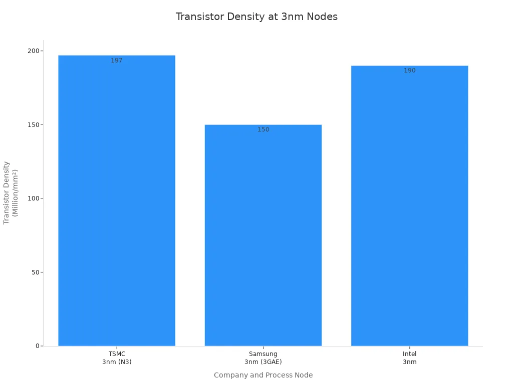
Intel’s 4 process node achieves 123 million transistors per mm², doubling the density of its predecessor and offering up to 40% lower power at the same frequency. As devices shrink below 3nm, quantum effects like electron tunneling increase leakage currents and heat, challenging reliability. The industry addresses these issues with advanced lithography, new materials, and 3D integration techniques. These innovations enable continued scaling, but also require new design and manufacturing strategies.
New Materials: Gallium Nitride and Silicon Carbide
Gallium nitride (GaN) and silicon carbide (SiC) are revolutionizing power electronics and RF applications. These wide-bandgap materials outperform traditional silicon by enabling higher power density, faster switching, and greater efficiency. GaN’s high electron mobility and breakdown voltage allow for rapid switching and compact designs, making it ideal for DC/DC converters, inverters, and RF amplifiers. SiC excels in high-voltage and high-temperature environments, supporting electric vehicle powertrains, renewable energy inverters, and industrial drives.
GaN transistors operate efficiently at frequencies up to 100 GHz, supporting 5G telecommunications and military radar systems. SiC devices handle voltages above 600 V and temperatures beyond 150°C, improving efficiency by 5-10% over silicon and reducing cooling requirements. The market for GaN devices is projected to grow from $7.8 billion in 2025 to $18.2 billion by 2030, driven by automotive, aerospace, and data center applications.
GaN and SiC enable smaller, lighter, and more efficient power systems, supporting the next generation of electric vehicles, renewable energy, and high-frequency communications.
Chiplet and Modular Design
Chiplet and modular design approaches break complex semiconductor systems into smaller, reusable components called chiplets. This strategy enables flexible integration, scalability, and rapid product development. Designers can mix and match chiplets for specific applications, combining different process nodes and specialized functions to optimize performance and cost.
- Chiplet technology supports faster time-to-market by allowing independent optimization and reuse of components.
- Standardization efforts like Universal Chiplet Interconnect Express (UCIe) promote interoperability and accelerate development.
- Advanced packaging methods such as 2.5D and 3D stacking maintain high bandwidth and low latency between chiplets.
- Industry leaders like AMD, Intel, and Qualcomm use chiplet architectures to improve scalability and power efficiency.
However, chiplet design introduces challenges in co-design, testing, thermal management, and security. Advanced interconnects and packaging technologies are essential to maintain performance and reliability in high-performance computing systems.
Backside Power Delivery and Energy Efficiency
Backside power delivery (BPD) is a breakthrough that enhances energy efficiency in advanced semiconductor devices. By relocating the power delivery network to the backside of the silicon wafer, BPD enables larger, less resistive power interconnects. This reduces voltage droop and power loss, providing a stable power supply to transistors and allowing higher operating frequencies.
BPD also frees up frontside space for signal routing, reducing congestion and improving signal speed. Technologies like through-silicon vias (TSVs) and wafer-level packaging support efficient vertical power delivery. Intel’s PowerVia technology demonstrates up to 30% reduction in power loss and a 15-20% decrease in power consumption at certain nodes. These improvements are critical for AI, 5G, and high-performance computing, where energy efficiency and thermal management are top priorities.
AI-Driven and “Shift-Left” Chip Design
AI-driven and “shift-left” methodologies are transforming chip design by automating and optimizing key stages of the process. AI analyzes past design patterns to optimize logic, placement, and routing, balancing area, power, and timing constraints. Neural networks and genetic algorithms automate layout generation, reducing manual effort and accelerating timelines.
- AI-driven verification detects design weaknesses early, improving reliability and shortening verification cycles.
- The “shift-left” approach incorporates early signal integrity analysis, reducing costly late-stage fixes.
- AI tools can accelerate design tasks up to ten times faster than traditional methods, supporting rapid innovation.
- These methods enable scalable, flexible design for complex multi-die and heterogeneous integration projects.
Challenges remain, such as data quality and integration with existing tools, but hybrid AI-traditional approaches show promise for future improvements.
Digital Twin Technology in Manufacturing
Digital twin technology creates virtual replicas of semiconductor fabs, equipment, and processes. These digital models enable real-time simulation, monitoring, and optimization, improving yield and reducing defects.
- Self-aware tools monitor manufacturing processes and detect potential failures in real time.
- Predictive maintenance reduces downtime and increases productivity by anticipating equipment issues.
- Virtual builds and simulations identify design issues early, speeding development and lowering costs.
- AI-powered digital twins provide actionable insights for process optimization, quality control, and resource use.
- Tool-level digital twins, such as Applied Materials EcoTwin™, autonomously monitor and adjust equipment to optimize wafer processing.
Hitachi High-Tech’s metrology solutions measure critical dimensions inline, supporting process control and reducing yield loss. Digital twins are deployed at multiple levels, from run-to-run control to predictive maintenance, supporting autonomous fabs and efficient decision-making.
Digital twin technology accelerates product development, improves quality, and supports the complex manufacturing needs of advanced semiconductor applications.
Semiconductor Applications in AI and High-Performance Computing

Accelerating Machine Learning and Generative AI
Data centers now rely on advanced semiconductor technologies to speed up machine learning and generative AI tasks. Companies like NVIDIA and Intel lead this transformation with specialized chips. The table below highlights how different technologies contribute to faster AI workloads:
| Technology/Company | Contribution to Faster Machine Learning and Generative AI Workloads |
|---|---|
| NVIDIA GPUs (A100, H100 Tensor Core) | Accelerate generative AI tasks such as deep learning, computer vision, and NLP. |
| Intel Xeon Scalable processors and AI chips (Nervana, Habana Labs) | Optimized for deep learning and AI workloads in data centers. |
| TSMC (5nm and 3nm process nodes) | Enables production of high-performance, energy-efficient AI chips for data centers and mobile devices. |
| AI-integrated semiconductors in data centers | Enhance server efficiency by speeding up ML functions, improving data access, and optimizing resource use. |
| AI-driven power management | Chips that dynamically adjust power consumption to improve energy efficiency and cooling in data centers. |
AI-specific GPUs and TPUs provide the high computational power needed for large models like GPT-4. Advanced process nodes, such as 5nm and 3nm, allow chips to run faster and use less energy. AI accelerators and NPUs handle real-time processing, making AI applications more efficient. These advances in semiconductor applications help data centers support the growing demand for AI.
High-Bandwidth Memory and Cloud Integration
High-Bandwidth Memory (HBM) changes how cloud-based AI and high-performance computing (HPC) systems operate. HBM uses stacked memory connected by through-silicon vias, which reduces latency and increases bandwidth. This design allows processors to access large amounts of data quickly, supporting massive parallel processing.
- HBM delivers higher bandwidth than traditional memory, which is essential for training and running large AI models.
- Advanced packaging, such as 2.5D integration, improves memory density and power efficiency.
- Lower power consumption per bit transferred helps reduce energy costs in large data centers.
- Custom HBM solutions, like those from Marvell, offer up to 25% more compute capacity and 70% lower interface power.
Meta’s Llama 3 infrastructure uses thousands of GPUs with HBM3, achieving high efficiency and saving millions in electricity costs. These features make HBM a key technology for cloud providers and hyperscalers, helping them overcome memory bottlenecks and scale AI workloads.
Semiconductor Applications in Automotive and Mobility

Powering Autonomous Vehicles and Advanced Driver Assistance Systems
Automotive technology now relies on advanced semiconductor innovations to enable safer and smarter vehicles. Companies design specialized chips to process large amounts of sensor data and make real-time decisions. The table below highlights key innovation areas and leading examples:
| Innovation Area | Description | Examples / Companies |
|---|---|---|
| Advanced Processing Power | Chips with high processing power handle complex algorithms and sensor data fusion. | Tesla HW4, NVIDIA DRIVE Orin, Mobileye EyeQ6 |
| Sensor Fusion | Integration of LIDAR, radar, and cameras for better environment perception. | Tesla, Mobileye, NVIDIA |
| Real-Time Decision Making | Ultra-low latency chips enable immediate response in traffic scenarios. | Tesla FSD Computer, NVIDIA DRIVE Orin X |
| AI and Machine Learning | Chips support AI for object detection and autonomous control. | Mobileye EyeQ6, Qualcomm Snapdragon Ride Flex |
| Connectivity (5G, V2X) | Chips enable vehicle-to-everything communication for traffic management. | Qualcomm Snapdragon Ride, Bosch AEC platform |
| Safety and Security | Enhanced collision avoidance, cybersecurity, and fail-safe designs. | Bosch, Infineon, Mobileye |
| Energy Efficiency | Power management chips optimize battery use and smart charging. | Infineon microcontrollers, Bosch power chips |
| Automotive Compute Architectures | Centralized and zonal architectures help integrate semiconductor technology. | Industry-wide adoption |
These innovation areas help vehicles sense their surroundings, make quick decisions, and stay connected. Semiconductor Applications in this field improve safety, efficiency, and the driving experience.
Enhancing Electric Vehicle Performance and Charging
Electric vehicles (EVs) benefit from new semiconductor technologies that boost battery management and charging speed. Wide-bandgap materials like silicon carbide (SiC) and gallium nitride (GaN) allow higher voltages and faster switching. These properties reduce energy loss and heat, which helps EVs drive farther on a single charge. SiC modules also support fast DC charging by handling high voltages and reducing cooling needs. Modular charger designs use stacked SiC units for more power and reliability.
Semiconductors now enable accurate battery cell monitoring, which supports safer and more affordable battery types. Intelligent battery junction boxes improve communication and measurement, making battery systems more reliable. These advances allow EVs to use different voltage levels, giving automakers more flexibility in design. As a result, drivers experience faster charging, longer range, and improved safety.
Automakers rely on semiconductor innovations to deliver smarter, safer, and more efficient vehicles for the future of mobility.
Semiconductor Applications in IoT and Smart Devices
Ultra-Low Power Chips for Billions of Connected Devices
Ultra-low power chips drive the rapid expansion of IoT and smart devices. These chips use advanced power management and energy harvesting to extend battery life and reduce maintenance. Key advancements include:
- Energy harvesting technologies allow devices to recharge from ambient sources like light, heat, or radio waves, supporting sustainable operation.
- Power management techniques such as subthreshold design, adaptive voltage scaling, power gating, and sleep modes minimize energy use.
- New materials, including gallium nitride (GaN) and silicon carbide (SiC), improve efficiency and reliability.
- Companies like e-peas create integrated circuits that manage energy harvesting and power, reducing the need for battery replacements.
- IoT microchips now feature adaptive power management and edge processing, which lower energy consumption and support longer device lifespans.
These innovations help billions of IoT devices operate longer on limited power, reducing costs and supporting environmental sustainability.
Secure and Scalable Connectivity Solutions
Security and scalability remain top priorities for IoT networks. Modern semiconductor solutions integrate hardware-based security features, such as secure enclaves and hardware roots of trust with unique device IDs. These features enable secure authentication and encrypted communication, protecting data and devices from unauthorized access. AI-driven anomaly detection and predictive threat mitigation provide adaptive responses to emerging threats at the network edge.
A hardware root of trust ensures each device can be uniquely verified, preventing spoofed devices from joining the network. Integrated iSIM solutions combine secure SIM operating systems, hardware roots of trust, and remote provisioning. This approach delivers flexible, scalable, and secure cellular connectivity for a wide range of IoT applications, from small sensors to industrial systems.
Semiconductor Applications in Telecommunications: 5G and 6G
High-Speed, Low-Latency Network Enablement
Telecommunications networks now depend on advanced semiconductor technologies to deliver the speed and reliability users expect from 5G and future 6G systems. Engineers use specialized RF transceivers, application processors, and FPGAs to process high-frequency signals and adapt in real time. These components help networks achieve ultra-high speeds and extremely low latency.
- Gallium nitride (GaN) and silicon carbide (SiC) materials allow devices to operate at higher frequencies and with greater power efficiency, which is essential for 6G.
- Integrated photonics combine light and electronic circuits on a single chip, increasing bandwidth and reducing signal loss.
- Neuromorphic computing chips, inspired by the human brain, support faster decision-making for complex network tasks.
- Antenna-in-package (AiP) technology places antennas directly in semiconductor packages, improving performance for mmWave and sub-terahertz communications.
These innovations help networks reach data rates beyond 1 Tbps and latency close to zero, supporting new applications like real-time remote surgery and autonomous systems.
Supporting Massive Device Connectivity
Next-generation networks must connect billions of devices, from smartphones to industrial sensors. Semiconductor Applications address this challenge with several key advancements:
- GaN-on-Si RF transistors provide high gain and efficiency at low voltages, which is critical for 6G and mmWave amplifiers.
- System-on-Chip (SoC) designs integrate processors, memory, and RF components, making devices smaller and more powerful.
- Advanced manufacturing nodes, such as 3nm and sub-5nm, enable AI-driven processors that manage large data loads.
- Low-power semiconductors extend battery life for IoT devices, while robust security features protect sensitive data.
- Improved thermal management and signal filtering maintain reliable connections, even as device density increases.
These developments ensure that future networks can handle massive connectivity, high data speeds, and complex processing needs.
Sustainable Semiconductor Applications and Green Technologies
Reducing Energy Consumption in Chip Production
Chip manufacturing uses large amounts of energy. Companies now focus on making these processes more efficient to lower environmental impact. They optimize steps like diffusion, etching, and lithography to use less power. Many fabs adopt energy-saving techniques from data centers, such as better HVAC and water systems. More factories use renewable energy sources to run their operations.
Manufacturers also extend chip lifetimes by improving cooling and recycling, which increases the energy return on investment. They use precise nitrogen dosing to cut down on waste and energy use. Energy-efficient components help reduce power needs in cleanrooms. Piezo technology lowers nitrogen consumption, which decreases CO₂ emissions while keeping quality high.
Key energy-saving methods include:
- Improving equipment efficiency in lithography, etching, and deposition.
- Using materials with lower greenhouse gas footprints.
- Optimizing nitrogen use in inert environments.
- Facility-wide upgrades for HVAC and water systems.
These strategies help reduce the carbon footprint of chip production and support a cleaner future.
Supporting Renewable Energy and Smart Grids
Semiconductor Applications play a vital role in renewable energy and smart grid systems. Modern chips enable efficient power conversion, energy storage, and grid integration. The table below shows how different semiconductor technologies support these areas:
| Semiconductor Technology | Role in Renewable Energy and Smart Grids |
|---|---|
| IGBT | Fast switching in inverters for solar and wind, converting DC to AC for grid use. |
| Wide Bandgap (SiC, GaN) | Operate at high temperatures and frequencies, reducing energy losses in EV charging and energy systems. |
| Silicon MOSFET | Manage power in solar inverters, EV chargers, and storage systems for stable electricity flow. |
| Power Management ICs | Monitor and control renewable energy systems, improving efficiency and reliability. |
| Energy Harvesting PMICs | Capture ambient energy, enabling self-powered devices and less battery waste. |
Smart grids use these technologies to balance energy supply and demand. They enable smart charging for electric vehicles and automate energy use in homes and offices. Countries like Thailand and states like New York invest in grid modernization to handle renewable energy and improve reliability. These advances make energy systems more flexible, efficient, and sustainable.
Overcoming Challenges in Semiconductor Applications
Addressing Supply Chain Shifts and Talent Shortages
Semiconductor companies face ongoing supply chain disruptions and a shortage of skilled workers. Many manufacturers report revenue losses and higher costs due to labor shortages. Companies respond by offering higher salaries and overtime, which increases wage bills. To reduce reliance on external skilled labor, they use simulation software and upskill existing staff.
Key strategies include:
- Reshoring manufacturing and diversifying supplier bases to improve resilience.
- Building workforce development programs with schools, government, and private partners.
- Adopting automation and AI to boost efficiency and reduce the need for scarce talent.
- Upskilling and reskilling employees to work with advanced technologies.
- Focusing on sustainability and ethical sourcing to meet regulations and customer expectations.
- Collaborating through apprenticeships, bootcamps, and joint training centers to bridge the skills gap.
Navigating Economic and Geopolitical Pressures
Economic and geopolitical factors shape the global semiconductor industry. The table below highlights recent trends:
| Aspect | Details |
|---|---|
| TSMC Market Share | 62% of foundry revenue in Q1 2024 |
| US Government Funding | Billions in grants and loans to Intel, TSMC, and Samsung for US fabs |
| China Investment | $47.5B state fund for semiconductor self-sufficiency |
| EV Sales (2024) | 15.2 million globally; China leads in battery electric vehicles |
| AI Chip Market Growth | Projected 29.4% CAGR to £496.9B by 2032 |
The US and China invest heavily in domestic production and technology leadership. Export controls and supply chain risks drive companies to diversify manufacturing locations. Europe also increases subsidies and investments to strengthen its sector. These pressures encourage innovation and a focus on resilience.
Advancing Environmental Sustainability
The industry works to reduce its environmental impact. Companies adopt processes that use fewer high global-warming potential gases and invest in emissions abatement technologies. They use sensing and automation to optimize raw material use and recycle water and process gases. Many factories now rely more on renewable energy. Government regulations and incentives push companies to adopt sustainability frameworks. Leading firms like Samsung, Intel, NXP, and Infineon show practical progress in these areas.
Semiconductor Applications continue to transform industries by enabling smarter devices, sustainable manufacturing, and rapid innovation.
- Experts predict strong growth in AI, automotive, and IoT, fueled by new materials and advanced packaging.
The industry’s focus on resilience and sustainability ensures connected technologies will evolve quickly, offering new opportunities for businesses and society.
FAQ
What industries benefit most from advanced semiconductor applications?
Automotive, telecommunications, healthcare, and consumer electronics see the greatest impact. These sectors use semiconductors to improve performance, safety, and connectivity.
How do new materials like GaN and SiC improve chip performance?
Gallium nitride (GaN) and silicon carbide (SiC) allow chips to run faster and cooler. These materials support higher voltages and frequencies, increasing efficiency.
Why is energy efficiency important in semiconductor design?
Energy-efficient chips lower power use, reduce heat, and extend device life. Companies save money and help the environment by using less electricity.