
TaC coating is a high-performance ceramic layer critical to advanced semiconductor manufacturing, particularly suited for SiC single crystal growth and GaN/SiC epitaxial processes. The rapidly expanding GaN/SiC semiconductor market is projected to reach US$7.523 billion by 2024, growing at a compound annual growth rate of 16.56% between 2025 and 2035.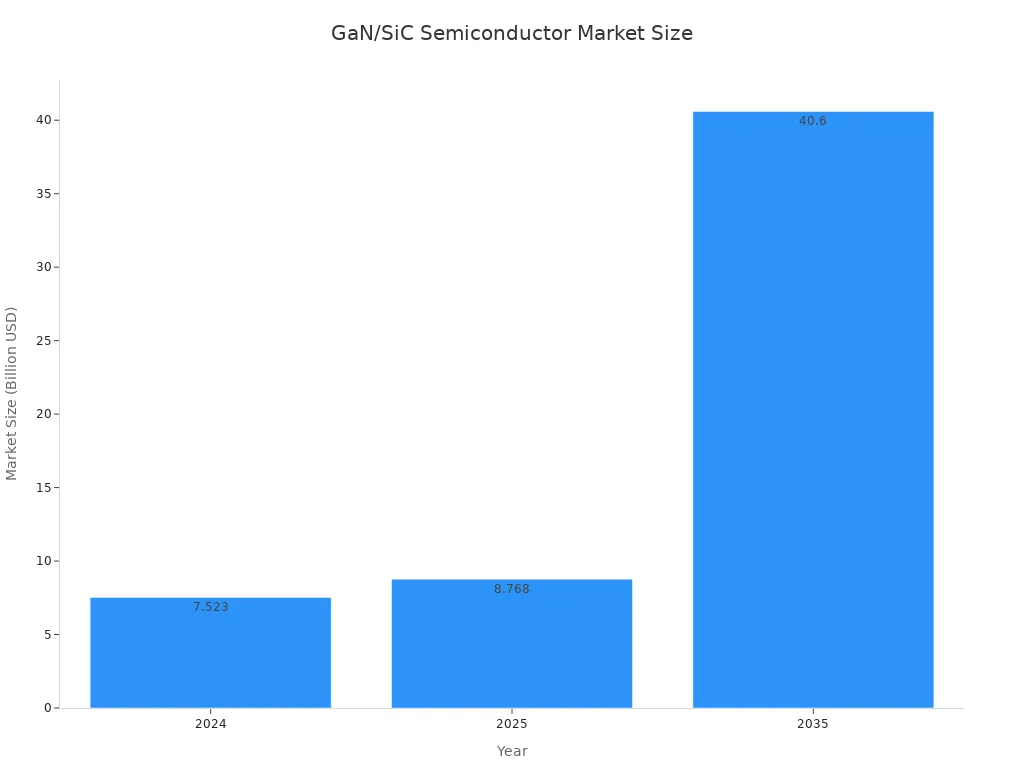
Tantalum carbide (TaC) is its primary chemical composition. Researchers study the Ta–C–N system, where TaC1-xNx represents the chemical composition. The base structure in experiments is the face-centered cubic (fcc) structure of Ta–C. Stable binary structures include fcc-TaC and hexagonal TaN (hex-TaN). For the cubic structure of Ta–C, non-metal vacancies are more critical than metal vacancies. Physical vapor deposition (PVD) can stabilize the fcc-structured Ta–C–N due to its highly constrained kinetics and the introduction of structural defects. In the TaC1-xNx system, a phase transition from single-phase fcc-Ta1-y-zCyNz to fcc + hexagonal Ta1-y-zCyNz occurs near x ≈ 0.68. Manufacturers prepare four different crystal structures of TaC coatings on carbon/carbon composites. These structures include an acicular crystal structure, which exhibits better ablation resistance.
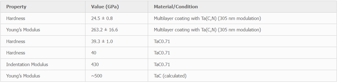
TaC coating is a specialized material that enhances computer chip performance, especially in high-temperature environments. It effectively prevents harmful substances from entering the chip, ensuring cleanliness and durability. Compared to other materials, TaC coating delivers superior performance, enabling higher-quality chip production and improved computer and smartphone functionality. Additionally, it exhibits exceptional mechanical properties, such as Ta(C,N) (305 nm modulation) multilayer coating with a hardness of 24.5 ± 0.8 GPa and Young’s modulus of 263.2 ± 16.6 GPa. TaC0.71 has a hardness of 39.3 ± 1.0 GPa, with some measurements reaching 40 GPa. Its indentation modulus is 430 GPa, while TaC’s calculated Young’s modulus is approximately 500 GPa.
The purity requirement for silicon carbide coatings exceeds 99.9995%, with the ability to withstand temperatures up to 1600°C. Its primary function is to isolate gaseous silicon and graphite, preventing reactions that generate silicon carbide particles and thereby avoiding wafer contamination. Given that silicon carbide constitutes a significant proportion of the cost in epitaxial crystal growth processes – accounting for over 40-50% of domestic crystal growth expenses – controlling the cost structure of silicon carbide crystal growth is paramount. Sustained material innovation and technological advancement are pivotal to overcoming industry challenges. Currently, graphite and silicon carbide ceramic materials are indispensable in semiconductor production, extensively utilised in critical components such as heaters, bases, crucibles, flow tubes, and connectors. The purity, chemical stability, and particularly the volatility of these materials directly impact the purity, performance, and quality of semiconductor materials.
Methods for preparing silicon carbide coatings include chemical vapour deposition (CVD), slurry pyrolysis, and plasma spraying. Among these, CVD technology is the most mature, yet it faces numerous technical limitations, high costs, and extended lead times.

