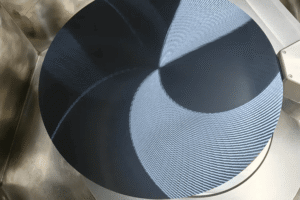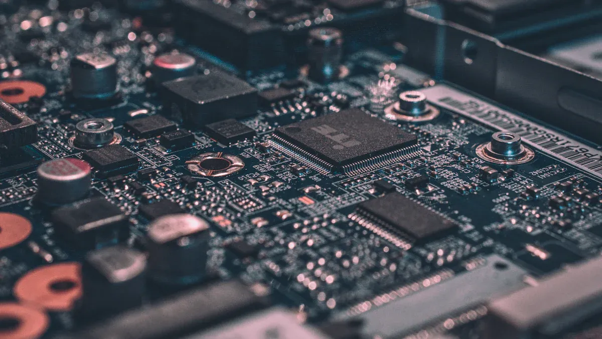
CVD SiC Layers stand out in modern technology. Engineers choose SiC Coating for its strength and resistance to heat. Silicon Carbide Coatings keep devices working in harsh places.
- Devices last longer and perform better with these layers.
- Next-generation electronics depend on their unique properties.
Key Takeaways
- CVD SiC layers provide strong heat resistance, chemical protection, and mechanical strength, making devices last longer and work better in tough conditions.
- These layers improve high-power electronics, sensors, and optical devices by enabling faster performance, better heat management, and durability in harsh environments.
- Advances in manufacturing and quality control help produce reliable CVD SiC layers at larger scales, opening new uses in electric vehicles, solar panels, and medical tools.
Unique Properties of CVD SiC Layers

Wide Bandgap and High Breakdown Voltage
CVD SiC Layers have a wide bandgap. This means they can handle high voltages without breaking down. Devices with these layers can work in strong electric fields. Engineers use them in power electronics because they stop unwanted current flow. Wide bandgap materials also help devices run faster and use less energy.
Devices with a wide bandgap can work in places where other materials fail. This property makes CVD SiC Layers important for advanced electronics.
Superior Thermal Stability and Conductivity
CVD SiC Layers show excellent thermal stability. They keep their shape and strength even at high temperatures. Many electronic devices heat up during use. These layers help move heat away from sensitive parts. Good thermal conductivity keeps devices cool and safe.
- High thermal stability means devices last longer.
- Good conductivity helps prevent overheating.
Chemical Resistance and Mechanical Strength
CVD SiC Layers resist many chemicals. They do not react easily with acids or bases. This property protects devices from damage in harsh environments. These layers also have strong mechanical strength. They can handle pressure and force without breaking.
| Property | Benefit |
|---|---|
| Chemical Resistance | Protects against corrosion |
| Mechanical Strength | Withstands physical stress |
CVD SiC Layers combine these properties to support reliable and long-lasting devices in both optics and electronics.
Main Applications of CVD SiC Layers in Electronics and Optics

High-Power and High-Frequency Electronic Devices
Engineers use CVD SiC Layers in high-power and high-frequency electronic devices. These layers help devices handle large amounts of electricity without overheating. Power converters, inverters, and radio frequency (RF) amplifiers often use this material. The wide bandgap and strong thermal properties allow these devices to work in tough conditions. Devices with these layers can run faster and last longer than those with traditional materials.
Note: Devices with CVD SiC Layers often show better energy efficiency and reliability in power electronics.
MEMS, Sensors, and Radiation-Hardened Electronics
Microelectromechanical systems (MEMS) and sensors need materials that can survive harsh environments. CVD SiC Layers protect these tiny devices from chemicals, heat, and radiation. Spacecraft and satellites use sensors with these layers because they resist damage from cosmic rays. Medical devices also benefit from this protection. The strong mechanical strength keeps MEMS working even under stress.
- MEMS with CVD SiC Layers can measure pressure, temperature, and movement.
- Sensors in nuclear plants use these layers to avoid radiation damage.
Photonic Devices, Waveguides, and Optical Detectors
CVD SiC Layers play a key role in photonic devices. These devices use light to send and receive information. Waveguides made with this material can direct light with little loss. Optical detectors with these layers can sense light in extreme environments. The wide bandgap helps these devices detect ultraviolet and visible light.
| Application | Benefit of CVD SiC Layers |
|---|---|
| Waveguides | Low signal loss |
| Optical Detectors | High sensitivity, durability |
| Photonic Devices | Stable performance |
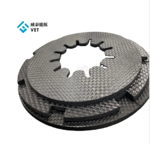
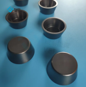
Protective Coatings and Diffusion Barriers
Many industries use CVD SiC Layers as protective coatings. These coatings shield parts from corrosion, wear, and chemical attack. In electronics, they act as diffusion barriers. This means they stop unwanted atoms from moving into sensitive areas. The layers keep devices safe and working longer.
- Factories use these coatings on tools and machine parts.
- Electronics makers use diffusion barriers to protect microchips.
Tip: Using CVD SiC Layers as coatings can lower maintenance costs and increase device lifespan.
Challenges and Innovations in CVD SiC Layers
Overcoming Fabrication Complexities
Manufacturers face many challenges when making CVD SiC Layers. The process needs high temperatures and special equipment. Small changes in temperature or gas flow can affect the final product. Engineers work to control these factors. They use advanced sensors and computer systems to watch each step. This helps them make layers that are smooth and even.
Note: Careful control during fabrication leads to better device performance.
Enhancing Material Quality and Scalability
Quality matters for every layer. Scientists test each batch for defects like cracks or uneven thickness. They use microscopes and lasers to check the surface. To make more layers at once, companies build bigger reactors. They also try new ways to grow layers faster without losing quality. These steps help lower costs and make CVD SiC Layers available for more uses.
- Quality checks prevent faulty devices.
- Larger reactors increase production.
Expanding Application Horizons
Researchers look for new ways to use these layers. They study how CVD SiC Layers work in new types of sensors and energy devices. Some teams test them in electric cars and solar panels. Others explore their use in medical tools and space missions. As more people learn about their benefits, the demand for these layers grows.
| New Application | Benefit |
|---|---|
| Electric Vehicles | Better heat management |
| Solar Panels | Improved durability |
| Medical Devices | High chemical resistance |
Researchers see these layers as a key part of new technology in optics and electronics. New methods help solve production problems. Many experts believe future devices will depend on these strong, reliable materials.
As technology grows, these layers will support safer and better-performing devices.
FAQ
What does CVD stand for in CVD SiC layers?
CVD stands for Chemical Vapor Deposition. This process creates thin, strong layers of silicon carbide on surfaces.
Why do engineers use CVD SiC layers in electronics?
Engineers use these layers because they resist heat, chemicals, and wear. Devices with CVD SiC layers last longer and work better in tough conditions.
Can CVD SiC layers improve optical devices?
Yes. CVD SiC layers help optical devices by making them more durable. They also allow these devices to work in high temperatures and harsh environments.
Tip: CVD SiC layers protect both electronic and optical devices from damage.