
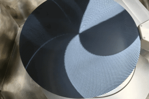
The Core Challenge: 1600°C and Beyond Growing high-quality epitaxial layers on 8-inch wafers requires an environment that is both chemically inert and thermally flawless. Any minor deviation in the susceptor’s surface or thermal conductivity can lead to fatal defects in the wafer.
At Vetek Semiconductor, we have refined our CVD SiC and TaC (Tantalum Carbide) coating technologies to meet these specific rigorous standards:
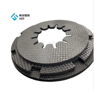
Precision Geometric Scaling: We ensure that the structural design and process requirements for our 8-inch susceptors remain perfectly consistent with proven 4-inch and 6-inch designs, allowing for a seamless transition in mass production.
Ultra-High Purity: Our base materials are strictly maintained at impurity levels below 5 ppm, ensuring zero contamination during the sensitive Epi-growth process.
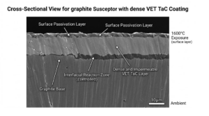
TaC Coating Advantage: For even more demanding environments (above 2000°C), our Tantalum Carbide coatings provide superior protection against hydrogen erosion, significantly extending the service life of graphite components.
A Technical Partnership for Long-term Value Manufacturing excellence in 2026 requires more than just a supplier; it requires a consultative partner who understands the physics behind the material. We focus on providing technical solutions that enhance yield and reduce downtime for our global partners.
Whether you are working with MOCVD, SiC Epitaxy, or Ion Implantation, our goal is to provide the material foundation that makes your next-generation chip designs a reality.
Connect for Technical Specifications: Detailed material data sheets, SEM cross-sections, and custom drawing evaluations are available upon request.

 Persian
  English
  Japanese
  German
  French
  Korean
  Arabic
  Portuguese
  Danish
  Spanish
  Finnish
  Indonesian
  Italian
  Russian