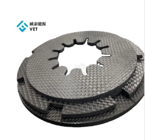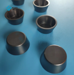
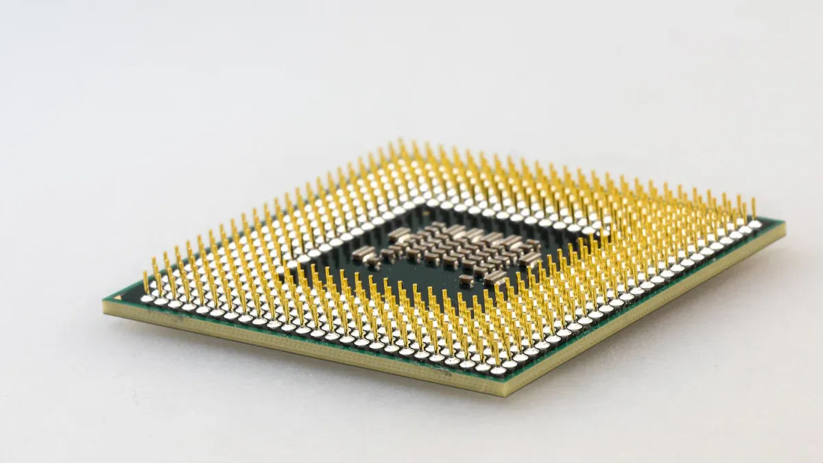
Ceramic Coatings are essential in the semiconductor industry, especially for 300mm silicon wafer processing. With outstanding attributes like plasma resistance and chemical inertness, they provide dependable performance for critical tools such as the EPI SUSCEPTOR and GRAPHITE SUSCEPTOR. Ningbo VET Energy Technology Co., Ltd leads advancements in CVD TAC COATING and CVD SIC COATING, boosting efficiency and longevity in wafer production processes.
Key Takeaways
- Advanced ceramic coatings help 300mm silicon wafer processing work better. They keep things stable under heat and stop wear, saving time and money.
- These coatings stop dirt in cleanrooms, keeping products pure and high-quality. This helps make better semiconductor devices.
- Using ceramic coatings saves money by making tools last longer. It also cuts down on repairs and upkeep for manufacturers.
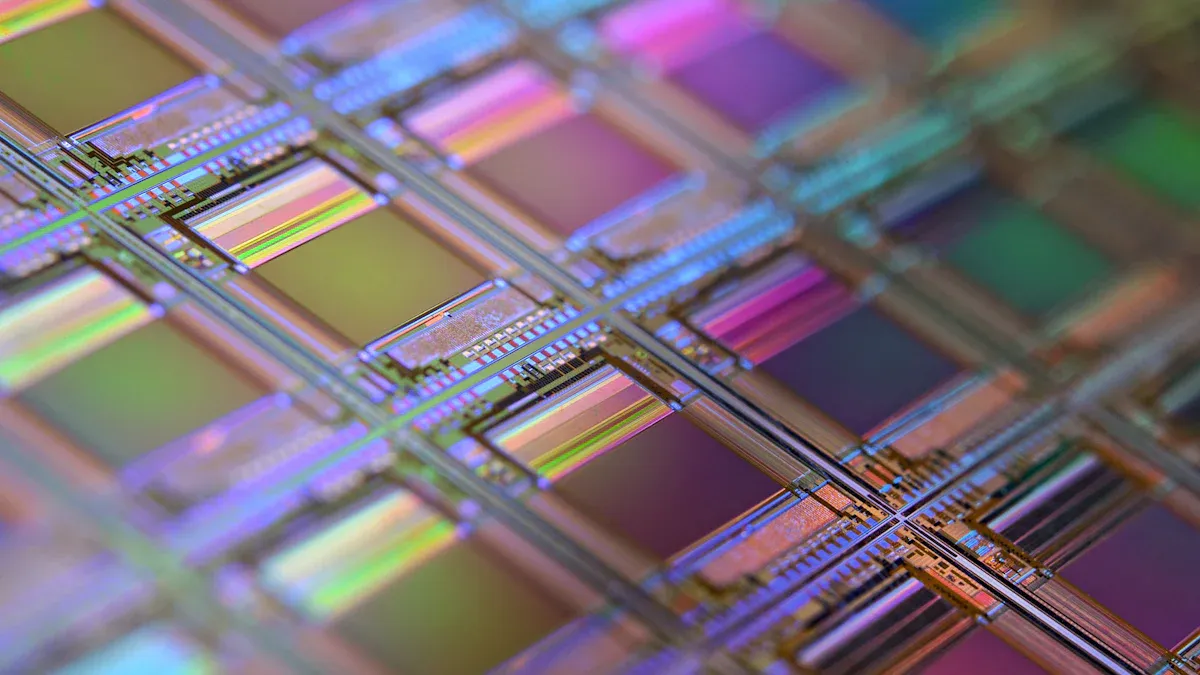
Understanding 300mm Silicon Wafer Processing
The significance of 300mm wafers in semiconductor manufacturing
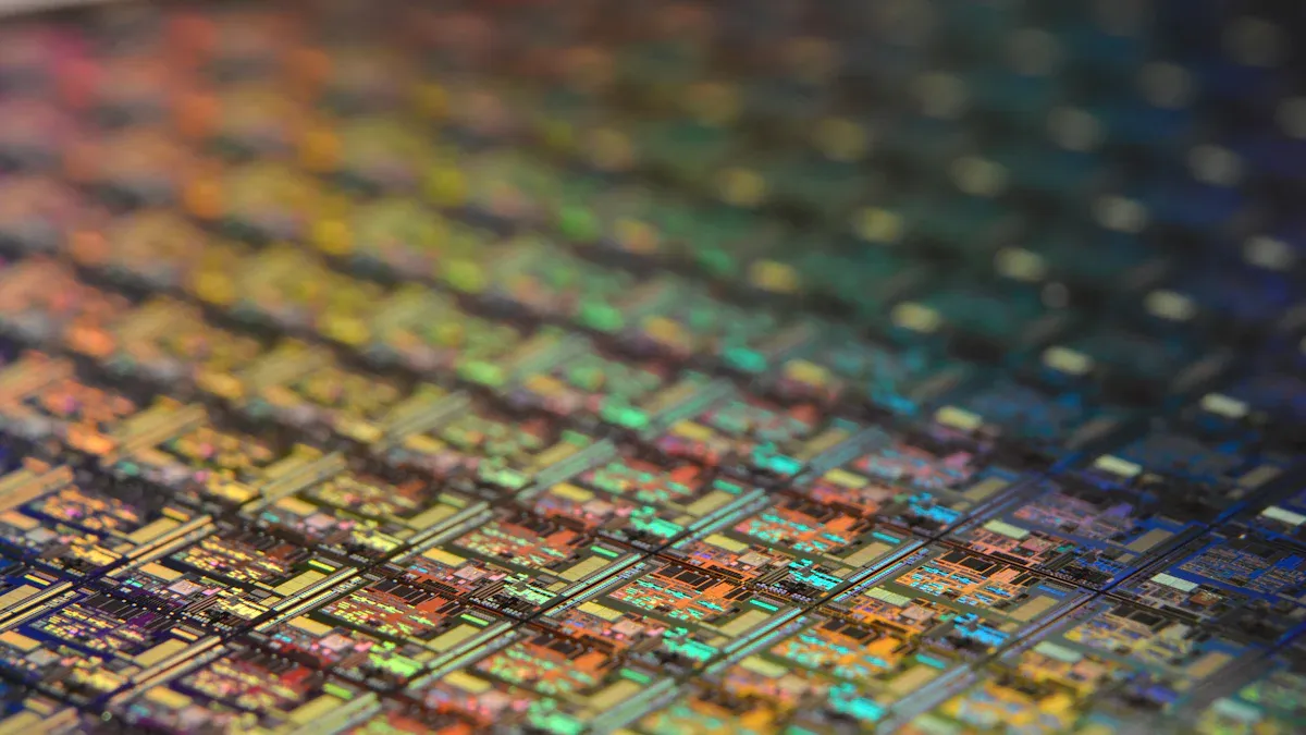
300mm silicon wafers have revolutionized semiconductor manufacturing by enabling higher efficiency and cost-effectiveness. These larger wafers allow manufacturers to produce more chips per wafer, significantly reducing production costs. For instance:
- A single 300mm wafer can accommodate 2.5 times the number of die compared to a 200mm wafer, resulting in a potential 30% reduction in unit integrated circuit (IC) costs.
- Leading companies like TSMC have adopted 300mm wafer technology since 2000, demonstrating its importance in modern semiconductor production.
The demand for 300mm wafers continues to grow due to their critical role in advanced technologies. The automotive industry relies on these wafers for producing components used in advanced driver assistance systems (ADAS) and autonomous vehicles. Similarly, consumer electronics, including smartphones and tablets, depend on 300mm wafers to support complex functionalities. Emerging technologies like 5G, artificial intelligence (AI), and the Internet of Things (IoT) further amplify the need for these wafers, making them indispensable for next-generation devices.
Challenges in processing large-diameter silicon wafers
Processing 300mm wafers presents unique challenges due to their size and complexity. Manufacturers must address issues such as thermal stress, mechanical damage, and surface quality to ensure optimal performance. The table below highlights some of the key challenges:
| Performance Metric | Challenge Description |
|---|---|
| Thermal Stress | Nonuniform temperature distributions cause dislocations and wafer distortion. |
| Mechanical Damage | Handling-induced microcracks and scratches reduce mechanical strength. |
| Surface Quality | Contamination and roughness impact lithography and electrical characteristics. |
| Dimensional Accuracy | Larger wafers require increased thickness to maintain strength and avoid damage during processing. |
Surface contamination remains a critical concern, as foreign particles can compromise flatness and cleanliness, leading to defects in integrated circuits. Additionally, mechanical damage, such as scratches or chipping, weakens wafer integrity, increasing the risk of breakage during manufacturing. Addressing these challenges is essential for maintaining the quality and reliability of 300mm wafers in semiconductor production.
Advanced Ceramic Coatings: Properties and Types
Key properties of ceramic coatings
Ceramic coatings play a vital role in semiconductor manufacturing due to their exceptional material properties. These coatings exhibit:
- Thermal Stability: Oxide ceramics can endure extreme temperatures, making them ideal for high-performance processes like chemical vapor deposition (CVD).
- Wear Resistance: Materials like alumina are renowned for their hardness and durability, ensuring longevity for tools and components exposed to abrasive conditions.
- Chemical Inertness: Oxide ceramics resist chemical reactions, which is critical for maintaining purity in semiconductor environments.
These properties enable ceramic coatings to withstand the demanding conditions of 300mm silicon wafer processing, ensuring consistent performance and reliability.
Types of ceramic coatings used in semiconductor applications
Different types of ceramic coatings serve specific purposes in semiconductor processing. The table below highlights key materials, their classifications, and usage scenarios:
| Ceramic Material | Classification | Usage Scenario |
|---|---|---|
| Silicon Dioxide (SiO2) | Insulating Material | Used as a gate dielectric in MOS devices and as an interlayer dielectric between metal interconnects. |
| Silicon Nitride (Si3N4) | Barrier Layer | Prevents metal diffusion into silicon substrates, maintaining device integrity. |
| Aluminum Oxide (Al2O3) | Protective Coating | Shields semiconductor devices from moisture and contaminants, also used as a gate dielectric. |
These coatings enhance the performance and durability of semiconductor devices. For instance, silicon nitride acts as a robust barrier layer, while aluminum oxide provides excellent protection against environmental factors. By leveraging these materials, manufacturers can optimize processes and improve product quality.
Applications of Ceramic Coatings in Wafer Processing
Thermal management in high-temperature processes
Ceramic coatings play a pivotal role in managing extreme temperatures during wafer processing. High-temperature processes, such as chemical vapor deposition (CVD) and plasma etching, demand materials that can endure intense thermal conditions without compromising performance. Ceramic coatings excel in this domain due to their exceptional thermal stability and resistance to degradation.
For instance, ceramic coatings can withstand temperatures up to 1200 °F (649 °C), making them indispensable for high-temperature applications. Their cross-linked siloxane structure enhances heat resistance, while silicone resins and robust pigments maintain stability under extreme conditions. Additionally, these coatings protect against corrosion, ensuring the integrity of tools and components exposed to harsh environments.
| Property | Description |
|---|---|
| Temperature Resistance | Ceramic coatings can withstand temperatures up to 1200 °F (649 °C), crucial for high-temperature applications. |
| Corrosion Resistance | They protect against corrosion, maintaining integrity under extreme conditions. |
| Stability Under Heat | Silicone resins and robust pigments remain stable under extreme heat, preventing degradation. |
| Cross-linked Structure | The siloxane bond forms a durable structure that enhances heat and chemical resistance. |
By leveraging these properties, manufacturers can ensure consistent thermal management, reducing the risk of wafer defects and improving overall process efficiency.
Wear resistance for critical equipment and tools
In semiconductor manufacturing, equipment and tools are subjected to abrasive conditions that can lead to wear and tear. Ceramic coatings provide a robust solution by significantly enhancing wear resistance, thereby extending the lifespan of critical components.
Research demonstrates that the performance of ceramic coatings depends on the combination of materials used. For example, coatings integrating WC–Co, NiCrBSi, and Cr3C2 exhibit superior wear resistance, with minimal wear depth observed under various conditions. This synergy between materials ensures durability and reliability in demanding environments. Furthermore, studies on TiB2/Cr multilayer coatings reveal that their innovative design reduces wear rates to just 30% of those seen in monolayer coatings. This improvement stems from enhanced toughness and resistance to crack propagation, making these coatings ideal for protecting tools and equipment.
By reducing wear, ceramic coatings minimize downtime and maintenance costs, enabling manufacturers to achieve higher throughput and operational efficiency.
Contamination prevention in cleanroom environments
Maintaining a contamination-free environment is critical in semiconductor fabrication. Even the smallest particles can compromise wafer quality, leading to defects in integrated circuits. Ceramic coatings address this challenge by providing a chemically inert and non-reactive surface that resists particle adhesion and contamination.
These coatings act as a protective barrier, shielding tools and components from chemical reactions and environmental pollutants. Their smooth, non-porous surfaces prevent the accumulation of debris, ensuring that cleanroom standards are upheld. Additionally, their resistance to chemical etching and plasma exposure further enhances their ability to maintain purity during wafer processing.
By preventing contamination, ceramic coatings contribute to higher yields and improved product quality, reinforcing their importance in semiconductor manufacturing.
Benefits of Advanced Ceramic Coatings
Enhanced efficiency and throughput in wafer processing
Advanced ceramic coatings significantly improve the efficiency of wafer processing by optimizing equipment performance. Their exceptional thermal stability ensures consistent operation during high-temperature processes, such as chemical vapor deposition (CVD) and plasma etching. This stability minimizes thermal fluctuations, which can otherwise lead to defects or delays in production.
For example, ceramic coatings maintain uniform heat distribution across wafer surfaces, reducing the risk of thermal stress and ensuring precise processing.
Additionally, their wear-resistant properties extend the lifespan of critical tools, reducing the frequency of replacements. This durability allows semiconductor manufacturers to maintain uninterrupted operations, leading to higher throughput. By enhancing process reliability, ceramic coatings enable manufacturers to meet the growing demand for advanced semiconductor devices efficiently.
Cost savings through reduced equipment wear and maintenance
The durability of ceramic coatings translates directly into cost savings for semiconductor manufacturers. Tools and components coated with these materials exhibit superior resistance to wear and tear, even under abrasive conditions. This resistance reduces the need for frequent repairs or replacements, lowering overall maintenance expenses.
A study on coated equipment revealed that ceramic-coated tools last up to three times longer than their uncoated counterparts. This extended lifespan minimizes downtime, as fewer interruptions occur for maintenance or part replacement. Furthermore, the chemical inertness of ceramic coatings protects equipment from corrosive substances used in wafer processing, further reducing repair costs.
By investing in ceramic coatings, manufacturers can achieve long-term savings while maintaining high operational efficiency.
Improved product quality and yield in semiconductor fabrication
Ceramic coatings play a crucial role in enhancing the quality and yield of semiconductor products. Their non-reactive surfaces prevent contamination during wafer processing, ensuring that the final products meet stringent purity standards. This contamination prevention is particularly vital in cleanroom environments, where even microscopic particles can compromise wafer integrity.
The smooth and uniform application of ceramic coatings also improves the precision of manufacturing processes. For instance, their ability to maintain dimensional accuracy during high-temperature operations ensures that wafers retain their structural integrity. This precision reduces the likelihood of defects, leading to higher yields and better overall product quality.
Manufacturers leveraging ceramic coatings can consistently produce reliable and high-performing semiconductor devices, meeting the demands of industries like consumer electronics, automotive, and telecommunications.
Future Trends in Ceramic Coatings for Next-Gen Wafer Processing
Innovations in coating materials and deposition techniques
Advancements in coating materials and deposition techniques are transforming the semiconductor industry. Researchers are developing ultra-thin coatings using nanotechnology to enhance thermal stability and mechanical stress resistance. These innovations improve the performance of tools and components in wafer processing.
Several companies are leading the way with cutting-edge technologies. For example:
| Company | Innovation | Description |
|---|---|---|
| Oerlikon Balzers | HiPIMS Technology | High-rate PVD capabilities for depositing thin films of metals, alloys, and ceramics. |
| Oerlikon Balzers | BALIQ TISINOS PRO | Enhances precision machining for hard materials, improving wear resistance and tool longevity. |
| AIXTRON | G10-SiC 200 mm Product Solution | Next-generation CVD system for large-scale SiC power device production on 150/200 mm wafers. |
These advancements ensure higher precision, durability, and efficiency in semiconductor manufacturing.
Integration with emerging technologies like EUV lithography
Ceramic coatings are becoming integral to emerging technologies such as extreme ultraviolet (EUV) lithography. EUV lithography requires materials that can withstand high-energy photon exposure while maintaining dimensional accuracy. Ceramic coatings provide the necessary thermal stability and wear resistance, ensuring reliable performance during these demanding processes.
The integration of real-time diagnostics in production processes further enhances the compatibility of ceramic coatings with EUV lithography. This technology allows manufacturers to monitor coating performance and address potential issues promptly, ensuring uninterrupted operations and higher precision.
Sustainability and eco-friendly advancements in ceramic coatings
Sustainability is a growing priority in semiconductor manufacturing. Ceramic coatings align with this trend due to their non-toxic and long-lasting properties. Recent advancements have introduced eco-friendly features, such as hydrophobic and antimicrobial properties, which enhance both performance and environmental benefits.
| Eco-Friendly Advancement | Description |
|---|---|
| Hydrophobic Properties | The TiO2-doped zinc phosphate coating exhibits superhydrophobicity with a contact angle of 153°, effectively preventing water ingress into porous substrates. |
| Antimicrobial Properties | The coatings demonstrate the ability to decompose organic and inorganic compounds, contributing to their antimicrobial effectiveness. |
| Environmental Benefits | Phosphate-based coatings provide material protection while also offering environmental advantages by repelling water and reducing corrosion. |
These innovations not only improve the durability of tools and components but also reduce the environmental impact of semiconductor manufacturing.
Advanced ceramic coatings play a pivotal role in addressing the challenges of 300mm silicon wafer processing. Their ability to enhance efficiency, reduce costs, and drive innovation makes them indispensable in semiconductor manufacturing.
Ningbo VET Energy Technology Co., Ltd remains at the forefront of ceramic coating advancements, shaping the future of high-performance semiconductor solutions.
FAQ
What makes ceramic coatings essential for 300mm silicon wafer processing?
Ceramic coatings provide thermal stability, wear resistance, and chemical inertness. These properties ensure reliable performance, reduce contamination, and enhance the durability of tools in semiconductor manufacturing.
How do ceramic coatings improve semiconductor manufacturing efficiency?
Ceramic coatings optimize equipment performance by reducing wear and thermal stress. This leads to fewer maintenance interruptions, higher throughput, and consistent wafer processing quality.
Why is Ningbo VET Energy Technology Co., Ltd a leader in ceramic coatings?
Ningbo VET Energy Technology Co., Ltd specializes in advanced CVD TAC and CVD SIC coatings. Their innovative solutions enhance efficiency, durability, and quality in semiconductor manufacturing processes.