
Epitaxial Epi Graphite Barrel Susceptor
Epitaxial Epi Graphite Barrel Susceptor is a specially designed support and heating device used to hold and heat semiconductor substrates during manufacturing processes like Deposition or Epitaxy processes.
Its structure includes typically cylindrical or slightly barrel-shaped, surface features multiple pockets or platforms for placing the wafers, can be solid or hollow design, depending on the heating method.
The main functions of epitaxial barrel susceptor:
1. Wafer Carrier and Temperature Control
The susceptor surface is designed with multiple wafer pockets (such as hexagonal or octagonal arrangement), which can support 6-15 wafers simultaneously. The high thermal conductivity of high-purity graphite (120-150W/m.K) ensures rapid heat transfer, combined with rotation function (5-20 RPM), resulting in a wafer surface temperature deviation of<± 1 ℃ and epitaxial layer thickness uniformity of<1%.
2. Optimization of reactant gas flow direction
The microstructure of the susceptor surface can break the boundary layer effect, allowing for uniform distribution of reaction gases (such as SiH4, NH3) and improving the consistency of deposition rate.
3. Anti pollution and anti-corrosion protection
Graphite substrates are prone to decomposition and release metal impurities (such as Fe,Ni) at high temperatures, while a 100μm thick CVD SiC coating can form a dense barrier to suppress graphite volatilization, resulting in a wafer defect rate of<0.1 defects/cm ².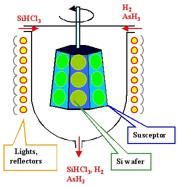
Applications:
- Primarily used for silicon epitaxial growth.
- Also suitable for epitaxy of other semiconductor materials like GaAs, InP, etc.
VET Energy utilizes high-purity graphite with CVD-SiC coating to enhance chemical stability:
1. High-Purity Graphite Material
High Thermal Conductivity: Graphite’s thermal conductivity is three times that of silicon, enabling rapid heat transfer from the source to the wafer, reducing heating time.
Mechanical Strength: Isostatic pressure graphite density ≥ 1.85 g/cm³, capable of withstanding temperatures above 1200℃ without deformation.
2. CVD-SiC Coating
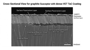
A β-SiC layer is formed on the graphite surface via chemical vapor deposition (CVD), with a purity of ≥ 99.99995%.
Coating thickness uniformity error is less than ±5%, and surface roughness is below Ra0.5μm.
3. Performance Enhancements
Corrosion Resistance: Withstands highly corrosive gases like Cl2 and HCl, extending GaN epitaxy lifespan by three times in NH3 environments.
Thermal Stability: Coefficient of thermal expansion (4.5 × 10⁻⁶/℃) matches graphite, preventing coating cracks from temperature fluctuations.
Hardness and Wear Resistance: Vickers hardness reaches 28 GPa, 10 times higher than graphite, reducing wafer scratch risks.

 Danish
  English
  Japanese
  German
  French
  Korean
  Arabic
  Portuguese
  Spanish
  Finnish
  Indonesian
  Italian
  Russian
  Persian