Why TaC Coating is a Game-Changer for High-Temp Nitrogen Processes

The Problem with Standard Coatings

Most coatings start to break down or “peel” when temperatures exceed 1600°C. In nitrogen-rich processes, this leads to:

  • Contamination of the wafer.

  • Frequent replacement of parts.

  • Higher production costs.
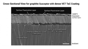
The TaC Solution

TaC is a “super-ceramic” with a melting point of 3880°C. Here is why it lasts longer in your reactor:

  1. Extreme Heat Resistance: It stays solid and stable far beyond the point where SiC coatings fail.

  2. Nitrogen Shield: TaC is chemically “lazy”—it doesn’t react with nitrogen. This prevents the coating from pitting or eroding over time.

  3. Perfect Match: It expands and contracts at the same rate as graphite, meaning no cracks during fast heating and cooling.

The Result: Lower Costs, Better Yields

By switching to TaC-coated parts, our clients see:

  • 2x to 3x longer part life.

  • Less downtime for maintenance.

  • Cleaner wafers and higher success rates.

Want to see the data? Visit us at www.cnvetenergy.com or message us directly to get the technical specs for your next project.

Condividere:

Altri post

Beyond Silicon: Why TaC Coating is Becoming the Gold Standard for 2000°C+ Environments

In the rapidly evolving power electronics landscape of 2026, we are pushing wide-bandgap semiconductors to their physical limits. As the demand for higher growth rates and superior crystalline quality intensifies, the industry is moving toward higher processing temperatures—often exceeding 2000°C. At these extremes, traditional materials fail, and Tantalum Carbide (TaC) coating emerges as the critical enabler.

Scaling Excellence: Solving Thermal Field Challenges in the 8-Inch SiC Era

In 2026, the semiconductor industry is no longer just a race for smaller nanometers; it is a race for material stability at extreme limits. As global production scales toward 8-inch Silicon Carbide (SiC) wafers to meet the demands of AI and high-voltage power electronics, the industry faces a critical bottleneck: Thermal Field Uniformity.

Navigating the 200mm Transition: Why TaC Coating is the Deciding Factor for 8-inch SiC Yields

Introduction As the global power electronics industry aggressively shifts from 150mm (6-inch) to 200mm (8-inch) SiC wafer production, the conversation often stays on the reactors themselves. However, at the heart of the MOCVD and Epitaxy process lies a silent but critical component: the graphite susceptor. If you are seeing a drop in yield or unexpected crystal defects as you scale to 8-inch, you aren’t alone. The thermal and chemical stresses at 1600°C+ are pushing traditional coatings to their breaking point.

The Endgame of 200mm SiC Scaling: Who Defines the Yield Ceiling in 2026?

As global leaders transition to total 200mm (8-inch) SiC production, the industry focus has shifted from “capacity” to “atomic-level control.” In the high-stakes environment of 2026, the real competition isn’t about wafer count—it’s about the coating technology that dictates your Fab’s bottom line.

Inviaci un messaggio

it_ITItalian

Looking forward to your contact with us

Let's have a chat