
O revestimento TaC é uma camada cerâmica de alto desempenho crítica para a fabricação avançada de semicondutores, particularmente adequada para crescimento de cristal único de SiC e processos epitaxiais de GaN/SiC. O mercado de semicondutores GaN/SiC em rápida expansão deverá atingir US$ 7,523 bilhões até 2024, crescendo a uma taxa composta de crescimento anual de 16,56% entre 2025 e 2035.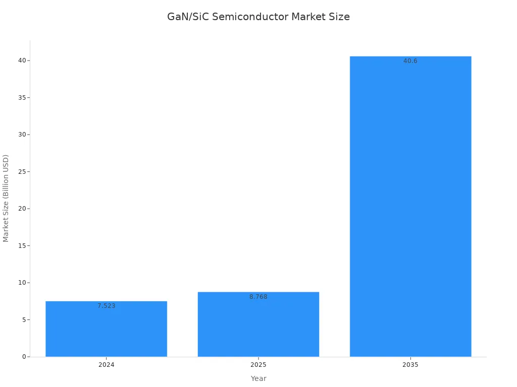
O carboneto de tântalo (TaC) é sua composição química primária. Os pesquisadores estudam o sistema Ta – C – N, onde TaC1-xNx representa a composição química. A estrutura base nos experimentos é a estrutura cúbica de face centrada (fcc) de Ta – C. Estruturas binárias estáveis incluem fcc-TaC e TaN hexagonal (hex-TaN). Para a estrutura cúbica de Ta – C, as vagas não metálicas são mais críticas do que as vagas metálicas. A deposição física de vapor (PVD) pode estabilizar o Ta – C – N estruturado em FCC devido à sua cinética altamente restrita e à introdução de defeitos estruturais. No sistema TaC1-xNx, uma transição de fase de fcc-Ta1-y-zCyNz monofásico para fcc + hexagonal Ta1-y-zCyNz ocorre próximo a x ≈ 0,68. Os fabricantes preparam quatro estruturas cristalinas diferentes de revestimentos de TaC em compósitos de carbono/carbono. Essas estruturas incluem uma estrutura cristalina acicular, que apresenta melhor resistência à ablação.
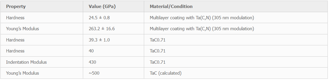
O revestimento TaC é um material especializado que melhora o desempenho do chip de computador, especialmente em ambientes de alta temperatura. Impede eficazmente a entrada de substâncias nocivas no chip, garantindo limpeza e durabilidade. Comparado a outros materiais, o revestimento TaC oferece desempenho superior, permitindo produção de chips de maior qualidade e melhor funcionalidade de computadores e smartphones. Além disso, apresenta propriedades mecânicas excepcionais, como revestimento multicamadas Ta(C,N) (modulação de 305 nm) com dureza de 24,5 ± 0,8 GPa e módulo de Young de 263,2 ± 16,6 GPa. TaC0,71 tem dureza de 39,3 ± 1,0 GPa, com algumas medições chegando a 40 GPa. Seu módulo de indentação é de 430 GPa, enquanto o módulo de Young calculado pelo TaC é de aproximadamente 500 GPa.
O requisito de pureza para revestimentos de carboneto de silício excede 99,9995%, com capacidade de suportar temperaturas de até 1600°C. Sua principal função é isolar o silício gasoso e o grafite, evitando reações que geram partículas de carboneto de silício e evitando assim a contaminação do wafer. Dado que o carboneto de silício constitui uma proporção significativa do custo nos processos de crescimento de cristais epitaxiais - representando mais de 40-50% das despesas domésticas de crescimento de cristais - é fundamental controlar a estrutura de custos do crescimento de cristais de carboneto de silício. A inovação sustentada de materiais e o avanço tecnológico são fundamentais para superar os desafios da indústria. Atualmente, os materiais cerâmicos de grafite e carboneto de silício são indispensáveis na produção de semicondutores, amplamente utilizados em componentes críticos como aquecedores, bases, cadinhos, tubos de fluxo e conectores. A pureza, a estabilidade química e particularmente a volatilidade desses materiais impactam diretamente a pureza, o desempenho e a qualidade dos materiais semicondutores.
Os métodos para preparar revestimentos de carboneto de silício incluem deposição química de vapor (CVD), pirólise de pasta e pulverização de plasma. Entre estas, a tecnologia CVD é a mais madura, mas enfrenta inúmeras limitações técnicas, custos elevados e prazos de entrega prolongados.