
Barco de Wafer Contíguo

VET enregy offer Barco de Wafer Contíguo base on semiconductor SIC and ceramic material. The special continuous structure design of the wafer boat ensures each wafer is tightly connected without gaps, maximizing space utilization and improving production efficiency. Precisely designed positioning holes ensure perfect alignment with fixtures during processing, enhancing accuracy and yield. Made of smooth, inert materials, the wafer boat prevents contamination, absorbs vibrations, and protects wafers during transport.

连续晶圆舟-3


Our State-Of-The-Art Manufacturing Facilities Offer:
• Ultra-high-purity recrystallized and CVD silicon carbides
• Advanced forming and casting technologies
• Extreme-precision CNC machining
• High-temperature firing capabilities
• Plasma coating technologies
• Advanced cleaning processes


Basic physical properties of Horizontal SiC Wafer Carrier:
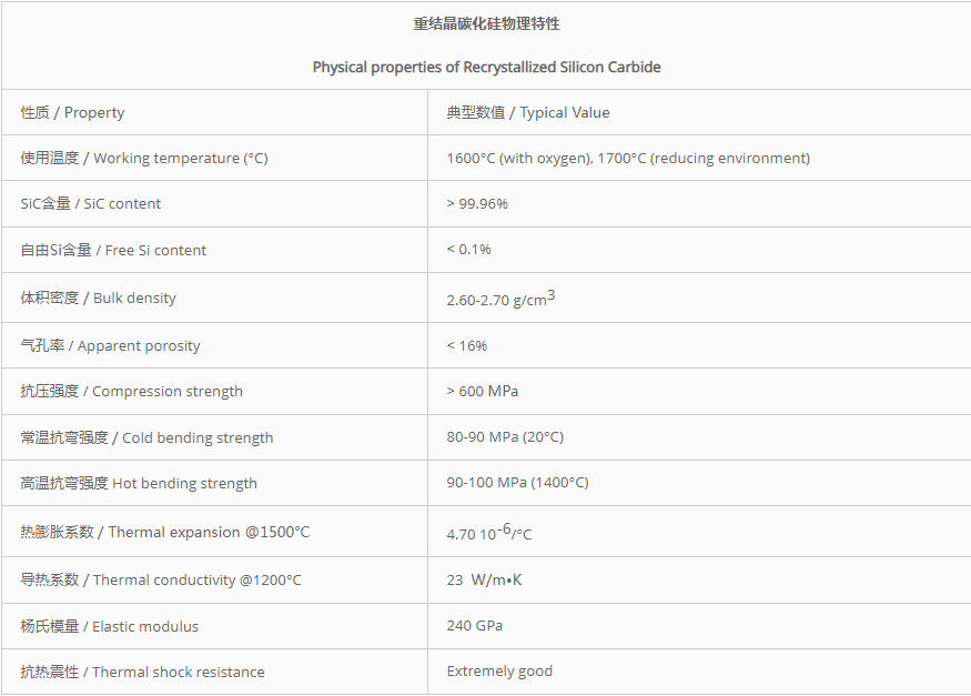


Advanced Material Research & Development
VET energy continues to make signficant investments in research and development to develop next-generation materials for the critical challenges faced by semiconductor and solar manufacturing industries. 


As a leading manufacturer and supplier of advanced coating materials in China’s semiconductor industry, VeT energy is committed to providing customers with various customized advanced technology and product solutions.We sincerely hope to become your long-term partner in China.
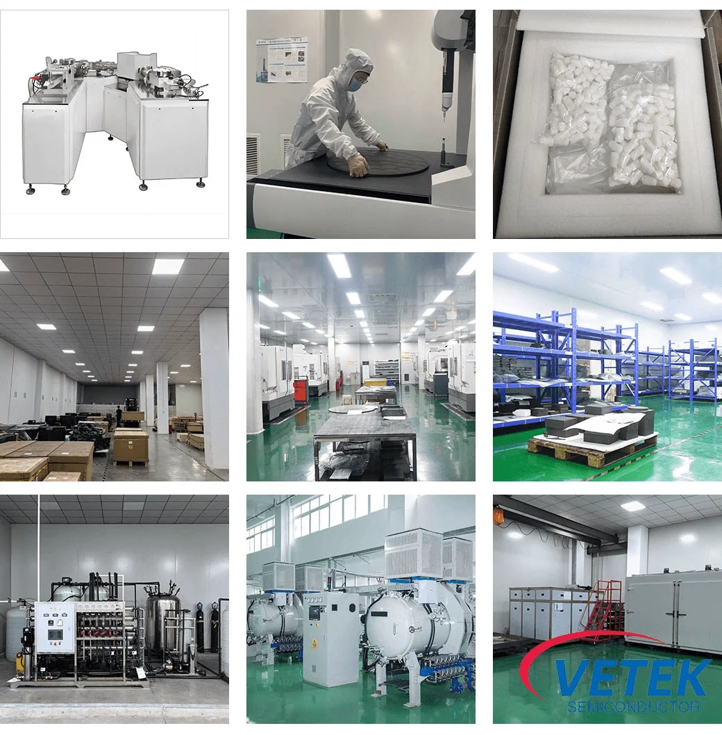
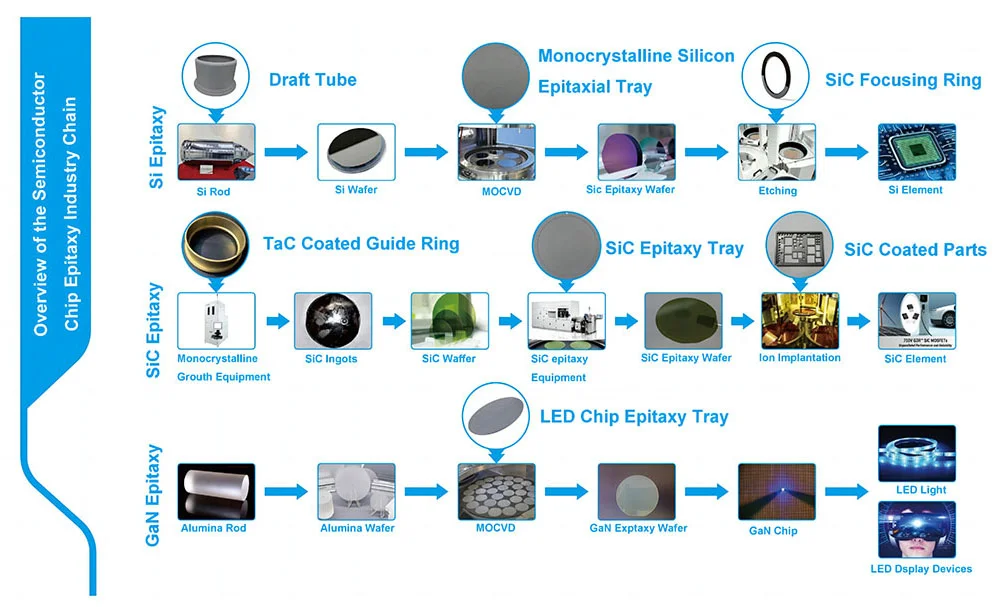
VeTek Semiconductor Wafer Boat shops


半导体芯片外延产业链概述

Partilha:

Mais Posts

The Zero-Particle Mission: Why Sub-5ppm Purity is the Foundation of Advanced Epitaxy

In 2026, as wide-bandgap semiconductors power everything from advanced AI servers to 800V automotive inverters, the margins for error have completely vanished. While chip designers push for higher efficiency, fab engineers face a daily battle against a microscopic enemy: contamination and micro-particles inside the process chamber. During high-temperature epitaxy, the standard of your graphite consumables directly dictates your final wafer defect density.

Maximizing ROI: The Financial Logic of Switching to TaC Coatings

In the competitive semiconductor landscape, the “initial purchase price” is often a misleading metric. For manufacturers scaling up to 8-inch SiC/GaN production, true profitability is found in Total Cost of Ownership (TCO).

At Vetek Semiconductor, we advocate for Carbido de tântalo (TaC) not just as a technical upgrade, but as a strategic financial decision to lower your Cost per Wafer.

Why TaC Coating is a Game-Changer for High-Temp Nitrogen Processes

In the world of semiconductor manufacturing, heat is the enemy of stability. As we move toward larger bolachas de 8 polegadas, traditional coatings are reaching their limits.

At Vetek Semiconductor, we’ve found that TaC (Tantalum Carbide) is the ultimate solution for longevity, especially in nitrogen (N2) environments.

Beyond Silicon: Why TaC Coating is Becoming the Gold Standard for 2000°C+ Environments

In the rapidly evolving power electronics landscape of 2026, we are pushing wide-bandgap semiconductors to their physical limits. As the demand for higher growth rates and superior crystalline quality intensifies, the industry is moving toward higher processing temperatures—often exceeding 2000°C. At these extremes, traditional materials fail, and Revestimento de carboneto de tântalo (TaC) emerges as the critical enabler.

Enviar uma mensagem

pt_PT_ao90Portuguese

Ansioso pelo seu contacto connosco

Vamos conversar

