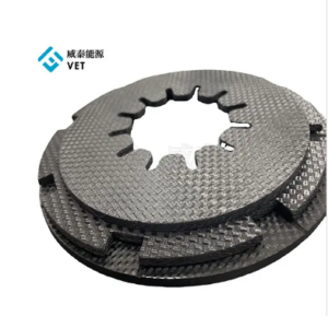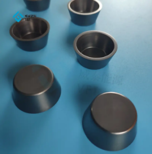
SiC Cantilever Paddles enhance semiconductor wafer handling by delivering exceptional thermal stability and precision. Their robust design minimizes contamination risks during high-temperature processes. Advanced manufacturing techniques, such as SIC COATING and CVD SIC COATING, rely on these paddles to achieve superior performance. Their integration ensures reliability and efficiency in critical semiconductor applications.
Key Takeaways
- SiC cantilever paddles help handle wafers better with great heat stability and accuracy, important for high-heat tasks.
- These paddles cut down contamination risks, improving wafer quality and reducing flaws, which makes production more efficient.
- Using SiC cantilever paddles saves money by lasting longer and needing less fixing, making them a smart choice for factories.
Overview of SiC Cantilever Paddles
Defining SiC Cantilever Paddles
SiC cantilever paddles are specialized tools designed for handling semiconductor wafers during high-temperature manufacturing processes. These paddles, made from silicon carbide, exhibit exceptional thermal and mechanical properties, making them indispensable in environments requiring precision and durability. Their cantilevered design allows for the safe and efficient transport of wafers, minimizing the risk of damage or contamination.
Key Properties of Silicon Carbide in Wafer Handling
Silicon carbide stands out due to its superior material properties compared to traditional materials. These properties ensure reliable performance in demanding semiconductor manufacturing environments.
| Property | Silicon Carbide (SiC) | Traditional Materials |
|---|---|---|
| Hardness | High | Moderate |
| Thermal Conductivity | Excellent | Lower |
| Thermal Expansion Coefficient | Low | Higher |
| Strength | High | Moderate |
These attributes enable SiC cantilever paddles to withstand extreme temperatures, maintain structural integrity, and reduce thermal stress on wafers.
Role of SiC Cantilever Paddles in Semiconductor Manufacturing
SiC cantilever paddles play a pivotal role in enhancing manufacturing precision and efficiency. They ensure the safe transport of wafers in high-temperature environments, preventing deformation and maintaining product quality. Their compatibility with automated handling systems supports large wafer loading capacities, streamlining production processes. Furthermore, their low thermal expansion coefficient aligns with LPCVD coatings, extending maintenance cycles and reducing contamination risks.
These paddles also find applications in photovoltaic cell manufacturing, demonstrating their versatility across industries. By integrating SiC cantilever paddles, manufacturers achieve higher yields, reduced defects, and improved operational efficiency.
Current Challenges in Semiconductor Wafer Handling
Addressing Fragility and Contamination Risks
Handling semiconductor wafers requires precision due to their fragility and susceptibility to contamination. Even minor mishandling can lead to edge defects or particle contamination, impacting wafer quality. Advanced wafer handling techniques, such as those utilizing SiC Cantilever Paddles, have significantly mitigated these risks. Their robust design ensures safe transport while minimizing contact points that could introduce contaminants.
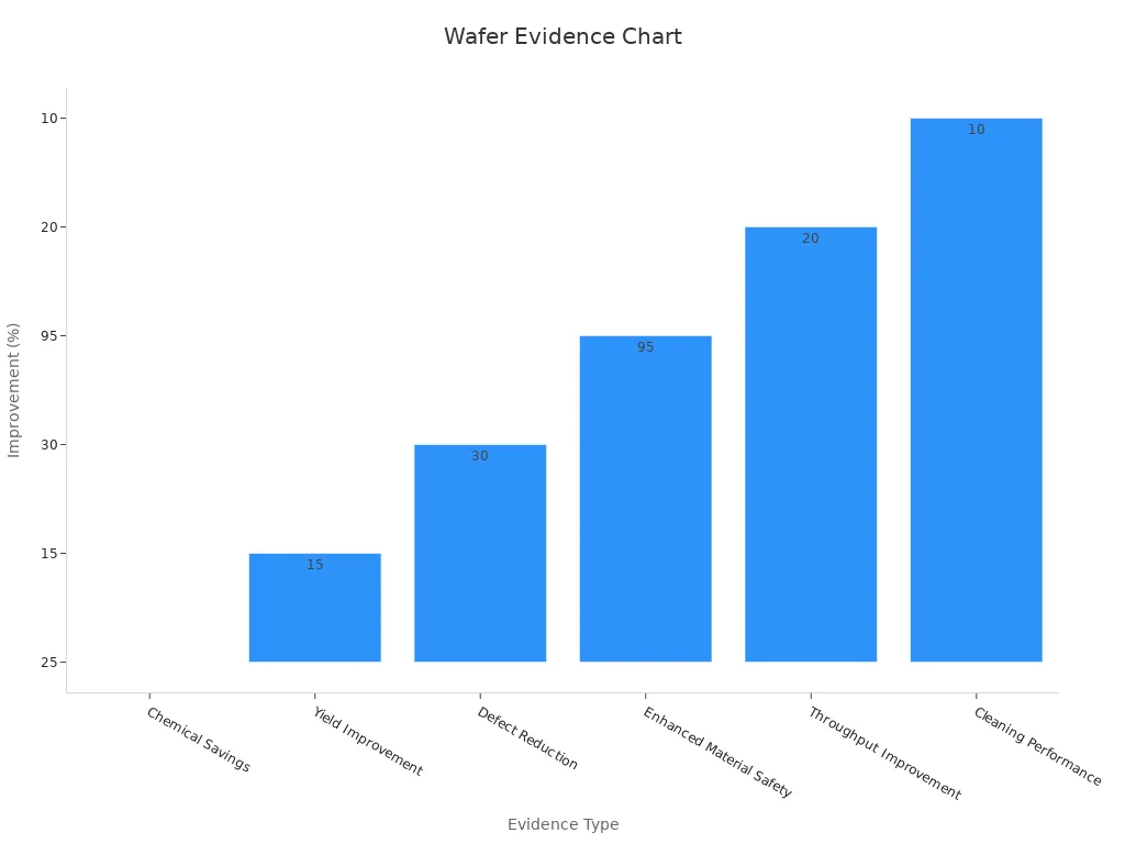
A study on wafer handling improvements highlights key advancements:
| Evidence Type | Result Description |
|---|---|
| Chemical Savings | Reduced chemical consumption by 25% without compromising cleaning quality. |
| Yield Improvement | Achieved a 15% increase in yield by ensuring uniform contaminant removal. |
| Defect Reduction | Decreased edge-related defects by 30%. |
| Enhanced Material Safety | Prevented over-etching in 95% of cases, protecting sensitive materials. |
| Process Consistency | Achieved uniform plasma coverage across all wafer edges. |
| Throughput Improvement | Increased throughput by 20% by eliminating scheduling delays. |
| Cleaning Performance | Enhanced cleaning uniformity, reducing particle defects by 10%. |
| Resource Efficiency | Improved chemical recycling efficiency, reducing costs and waste. |
Overcoming Thermal and Mechanical Stress
Semiconductor manufacturing involves extreme thermal and mechanical conditions. Traditional materials often fail to withstand these stresses, leading to deformation or reduced lifespan. SiC Cantilever Paddles excel in such environments due to their low thermal expansion and high mechanical strength. Simulation results demonstrate their effectiveness in stress management:
| Architecture | Stress Reduction (%) | Temperature Increase (%) | Wirelength Improvement (%) |
|---|---|---|---|
| Micro150 | 19.8 | Slightly Increased | N/A |
| MultiGPU | 7.8 | 0.39 | 5.2 |
Limitations of Traditional Materials in Precision Environments
Traditional materials like quartz and graphite often fall short in precision environments. Their higher thermal expansion coefficients and lower mechanical strength make them prone to warping and contamination. Silicon carbide, by contrast, offers superior thermal stability and durability. This makes it an ideal choice for applications requiring high precision and reliability, such as advanced lithography and etching processes.
Emerging Applications of SiC Cantilever Paddles

High-Temperature Wafer Processing
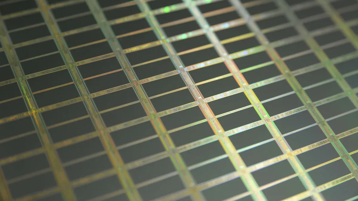
SiC cantilever paddles excel in high-temperature wafer processing, a critical stage in semiconductor manufacturing. Their exceptional thermal stability allows them to withstand extreme temperatures without warping or degrading. This property ensures consistent wafer alignment and reduces the risk of defects during processes such as oxidation and annealing. Manufacturers rely on these paddles to maintain precision in environments where traditional materials like quartz often fail. By integrating SiC cantilever paddles, production lines achieve higher throughput and improved wafer quality, making them indispensable in modern semiconductor fabrication.
Advanced Lithography and Etching
Advanced lithography and etching processes demand unparalleled precision and material integrity. SiC cantilever paddles meet these requirements by offering low thermal expansion and high mechanical strength. These attributes ensure that wafers remain stable during intricate patterning and etching stages. The paddles’ compatibility with cutting-edge lithography techniques, such as extreme ultraviolet (EUV) lithography, further enhances their utility. Their ability to minimize thermal distortion and contamination makes them a preferred choice for achieving nanoscale accuracy in semiconductor devices.
Contamination-Free Wafer Transport
Contamination-free wafer transport is essential for maintaining the integrity of semiconductor wafers. SiC cantilever paddles play a pivotal role in this area by significantly reducing impurity levels during wafer handling. Laboratory measurements confirm that CVD-SiC paddles consistently achieve impurity levels below 3.5 ppm, a stark contrast to traditional materials like quartz and Norton SiC, which exhibit impurity levels exceeding 35 ppm and 350 ppm, respectively.
| Material Type | Total Impurity Level (ppm) |
|---|---|
| CVD-SiC | < 3.5 |
| GE Quartz | > 35 |
| Norton SiC | > 350 |
These results highlight the superior performance of SiC cantilever paddles in maintaining a contamination-free environment. Their adoption ensures cleaner wafer surfaces, leading to higher yields and fewer defects in semiconductor manufacturing.
Applications in Next-Generation Materials (e.g., GaN, SiC)
The rise of next-generation materials like gallium nitride (GaN) and silicon carbide (SiC) has introduced new challenges in wafer handling. These materials require specialized processing conditions due to their unique thermal and mechanical properties. SiC cantilever paddles provide the necessary support for handling these advanced materials. Their high thermal conductivity and mechanical strength make them ideal for managing the demands of GaN and SiC wafer processing. By enabling precise and reliable handling, these paddles contribute to the development of high-performance devices such as power electronics and optoelectronic components.
Use in Photovoltaic Diffusion Coating Furnaces
Photovoltaic cell manufacturing involves diffusion coating processes that operate at extremely high temperatures. SiC cantilever paddles are well-suited for these applications due to their ability to maintain structural integrity under thermal stress. Their low thermal expansion coefficient ensures uniform coating distribution, which is critical for achieving optimal photovoltaic cell efficiency. Manufacturers have increasingly adopted these paddles in diffusion furnaces to enhance production reliability and reduce maintenance requirements. This application underscores the versatility of SiC cantilever paddles in supporting renewable energy technologies.
Benefits and Industry Impact
Enhanced Durability and Longevity
SiC cantilever paddles exhibit remarkable durability and longevity, making them indispensable in semiconductor manufacturing. Their silicon carbide composition allows them to endure extreme temperatures and resist harsh chemical environments. This resilience ensures consistent performance over extended periods, even in demanding applications. For instance, in photovoltaic production, these paddles maintain their structural integrity during high-temperature diffusion processes, reducing the need for frequent replacements. An industry report highlights the advanced properties of silicon carbide ceramics, emphasizing their ability to enhance the operational lifespan of tools in solar cell manufacturing. By leveraging these qualities, manufacturers achieve greater reliability and reduced downtime.
Improved Wafer Yield and Reduced Defects
The precision and stability of SiC cantilever paddles directly contribute to improved wafer yield and reduced defects. Their low thermal expansion coefficient minimizes thermal distortion, ensuring accurate wafer alignment during high-temperature processes. This precision reduces edge defects and contamination, which are common issues in semiconductor fabrication. Additionally, their contamination-free handling capabilities maintain wafer purity, leading to higher-quality outputs. By integrating these paddles into production lines, manufacturers can achieve a significant reduction in defect rates, ultimately enhancing overall yield.
Cost Efficiency in High-Volume Manufacturing
Cost efficiency is a critical factor in high-volume semiconductor manufacturing. SiC cantilever paddles offer a cost-effective solution by reducing maintenance requirements and extending tool lifespans. Their durability minimizes the frequency of replacements, lowering operational costs. Furthermore, their ability to withstand extreme conditions without degradation ensures consistent performance, reducing production interruptions. These factors collectively contribute to lower total cost of ownership, making them an economically viable choice for large-scale manufacturing facilities.
Enabling Advanced Semiconductor Technologies
The adoption of SiC cantilever paddles plays a pivotal role in enabling advanced semiconductor technologies. Their compatibility with cutting-edge processes, such as extreme ultraviolet (EUV) lithography and advanced etching techniques, supports the development of next-generation devices. These paddles provide the precision and stability required for nanoscale manufacturing, ensuring the production of high-performance components. As the semiconductor industry continues to push the boundaries of innovation, SiC cantilever paddles remain at the forefront, facilitating the realization of complex designs and architectures.
Contributions by Ningbo VET Energy Technology Co., Ltd
Ningbo VET Energy Technology Co., Ltd has emerged as a key contributor to the advancement of SiC cantilever paddles. The company leverages its expertise in silicon carbide material engineering to develop high-quality paddles tailored to the needs of the semiconductor industry. Their innovative manufacturing processes ensure superior thermal stability and mechanical strength, setting new benchmarks for performance and reliability. By collaborating with industry leaders, Ningbo VET Energy Technology Co., Ltd continues to drive innovation, enabling manufacturers to achieve higher yields and operational efficiency. Their commitment to excellence underscores their pivotal role in shaping the future of semiconductor wafer handling.
Future Trends and Research Directions
Innovations in SiC Material Engineering
Silicon carbide (SiC) continues to drive advancements in semiconductor applications through material engineering innovations. Researchers are exploring epitaxial growth techniques to enhance wafer quality and performance. Advanced packaging technologies are improving yields and enabling smaller, lighter components for consumer electronics. New materials like gallium nitride (GaN) and SiC are gaining prominence for their efficiency and durability, particularly in electric vehicles and renewable energy systems.
SiC’s role in emerging industries is expanding rapidly:
- Electric vehicles benefit from enhanced powertrain efficiency, enabling longer ranges and faster charging.
- Wireless communications leverage SiC for 5G networks and satellite systems.
- Renewable energy systems achieve improved power conversion efficiency, supporting sustainability goals.
Integration with Automation and Robotics
Automation and robotics are transforming semiconductor manufacturing, and SiC cantilever paddles are integral to this evolution. Their compatibility with automated systems ensures precise wafer handling, reducing human error and increasing throughput. AI-driven optimization in chip design and IoT integration are further boosting demand for energy-efficient SiC-based components. These technologies enable seamless operation in high-volume production environments, paving the way for ultra-fast communication and advanced semiconductor solutions.
Expanding Applications Beyond Semiconductors
SiC’s versatility extends beyond semiconductor manufacturing. NASA’s Glenn Research Center is developing SiC for aerospace applications, with devices operating at temperatures exceeding 500°C. SiCf/SiC composites are being researched for nuclear reactor fuel cladding, focusing on accident tolerance and enhanced material properties. These advancements highlight SiC’s potential in high-temperature environments, establishing its role in industries like aerospace, nuclear energy, and renewable technologies.
Research Initiatives by Ningbo VET Energy Technology Co., Ltd
Ningbo VET Energy Technology Co., Ltd is spearheading research in SiC material engineering. Their focus includes interface modification and preparation processes to optimize SiC properties for diverse applications. By exploring advanced techniques like chemical vapor infiltration (CVI) and polymer infiltration and pyrolysis (PIP), the company is enhancing the durability and thermal stability of SiC paddles. Their commitment to innovation positions them as a leader in shaping the future of SiC technology across industries.
SiC cantilever paddles redefine semiconductor wafer handling by delivering unmatched thermal stability, durability, and precision. Their adoption drives efficiency across industries, with projected growth exceeding 15% CAGR.
| Industry Sector | Projected CAGR | Impact on Manufacturing Efficiency |
|---|---|---|
| Semiconductor Sector | Significant | Improved performance and reduced energy consumption |
| Automotive Industry | > 20% | Increased demand for high-performance components in EVs |
Ningbo VET Energy Technology Co., Ltd continues to lead innovation, ensuring their widespread adoption and transformative impact.
FAQ
What makes SiC cantilever paddles superior to traditional materials?
Silicon carbide offers unmatched thermal stability, mechanical strength, and contamination resistance. These properties outperform traditional materials like quartz and graphite in semiconductor manufacturing.
How do SiC cantilever paddles improve wafer yield?
Their precision and low thermal expansion reduce defects and contamination. This ensures accurate wafer alignment, leading to higher yields in semiconductor production.
Why is Ningbo VET Energy Technology Co., Ltd significant in this field?
The company pioneers SiC material engineering, delivering innovative, high-quality paddles. Their contributions enhance manufacturing efficiency and drive advancements in semiconductor technologies.